- Original content, please do not reprint.
What is a field effect tube?
Field effect is an effect of long-distance polarity that can interact with each other, transmitting electron effects through spatial and solvent molecules. It can generate an electric
field within space through intramolecular electrostatic forces in space, affecting reaction centers at another location. The field-effect transistor is a semiconductor device that uses
such an electric field effect to control its current size. Its advantages include small size, light weight, low power consumption, simple packaging, few pins, and long lifespan. It has
many advantages, including high input impedance, low noise stability, strong radiation resistance, and more. Due to its very simple manufacturing process, the field-effect transistor
is highly economical and practical. Because of its wide range of applications, it can even withstand operation at 0-degree coefficient, making it widely used.

The working principle of the field effect tube
The field-effect transistor is a current-controlled element. It is also called a bipolar device because it can operate with both majority and minority carriers.
Classification of FET
Metal Oxide_Semiconductor FET | enhancement mode | N-channel |
| P-channel | ||
depletion mode | N-channel | |
| P-channel | ||
Junction-FET | N-channel | |
| P-channel |
Insulated gate field effect transistor
1、Insulated gate field effect transistor (Metal Oxide_Semiconductor FET), abbreviated as MOSFET
There are many kinds of insulated gate field effect transistors, such as PMOS, NMOS and VMOS power transistors, but MOS transistors are used most.
(Metal oxide semiconductor field effect transistor)
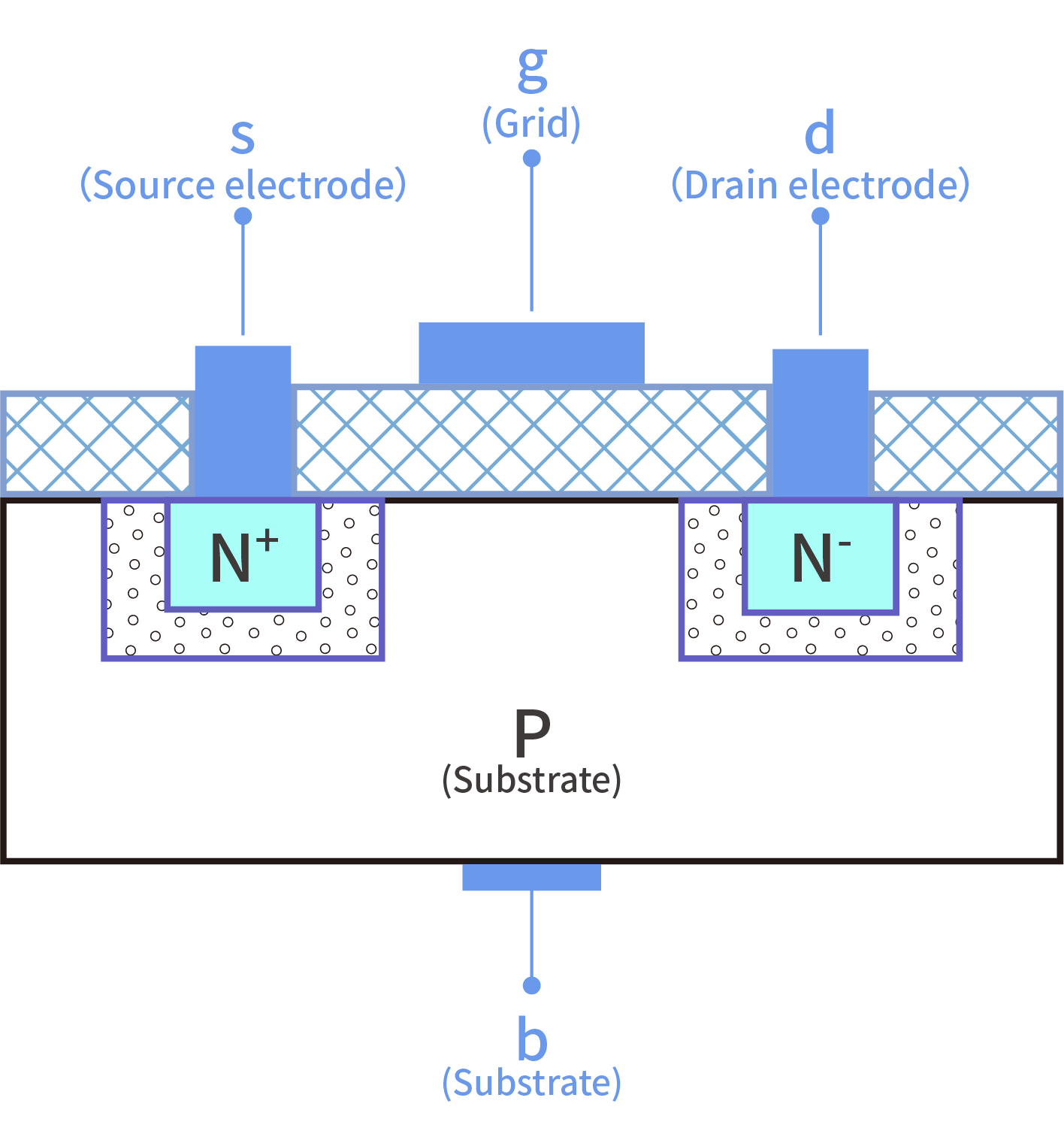
The schematic diagram and symbols of the structure of an N-channel enhanced MOSFET. It is formed on a P-type silicon substrate by diffusing two high-concentration N regions,
creating a thin layer of silicon dioxide (SiO2) insulating layer between the two N regions, and then drawing three electrodes—referred to as source s, gate g, and drain d—on the SiO2
and the two N regions. In its schematic symbol, the arrow indicates the actual direction of the drain current.
assumption diagram:


The conduction mechanism of an Insulated Gate Field Effect Transistor (IGFT) is to control the width of the conductive channel by adjusting the amount of "induced charge" using UGS,
thereby controlling the drain current ID. When UGS=0, there is no conductive channel between the source and drain, which is referred to as an enhancement MOSFET. When UGS=0,
there is a conductive channel between the drain and source, which is referred to as a depletion MOSFET
2、N-ChannelFET
(1)Static working principle of an N-channel MOSFET, this electronic device meticulously constructed from N-type material, when a
negative voltage (Vgs) is applied between the gate and source, it forms a uniform electric field between the gate and channel, thereby
creating a channel with a higher concentration of N-type carriers. This phenomenon significantly reduces the conduction resistance
between the drain and source, facilitating smooth current flow.

On the contrary, when the voltage between the gate and the source is zero (Vgs=0), the N-channel field-effect transistor is in the off
state. At this time, the carrier concentration in the channel is not enough to form an effective current channel, and the device behaves
as a high impedance state, which hinders the current through.
(2)Dynamic working principle
We can try applying a forward voltage between the drain and the source. By taking advantage of the lower potential energy at the
drain and the higher potential energy at the source, the resistance between them is very low, allowing current to flow from the drain
to the source. Of course, we can try applying more voltage Vds to further reduce the potential at the drain. At this point, the electron
concentration in the channel will decrease, and the resistance will increase. Eventually, when Vds reaches a certain value, the resistance
also increases, and the current will hardly increase any further, reaching a saturated state.
3、 P-ChannelFET
(1)Static working principle
The P-channel field-effect transistor, as its name suggests, is a device made of a P-type material. When the voltage Vgs between the
transistor and the source is positive. the electric field between the gate and the channel will be in a balanced state. At the same time,
there will be a higher concentration of P-type channels. This will also reduce the resistance between the source and the drain.

(2) Dynamic working principle
When a negative voltage (Vds) is applied between the drain and source, the potential at the drain is higher than that at the source.
Due to the low resistance between the drain and source, current flows from the source to the drain. As Vds increases, the potential at
the drain rises further, leading to a decrease in hole concentration in the channel and an increase in resistance. When Vds reaches a
certain specific value, the channel resistance significantly increases, and the current no longer changes much with voltage, entering a
saturation state. At this point, the current is referred to as IDSS, and the corresponding voltage is Vp.
The main parameters of the field effect tube
(1) On voltage UT (U is the parameter of MOS enhancement tube, the gate source voltage is less than the absolute value of the on voltage, the field effect tube cannot conduct)
(2) Break voltage Up Up is the parameter of MOs depletion and junction FET. When ucs = Up, the drain current is zero.
(3) Saturation drain current IDss MOS depletion and junction FET, the drain current corresponding to when ucs = 0.
(4) Input resistance Rcs Junction field-effect transistor, Re greater than 1079, MOS field-effect transistor, R can reach 10~10152.
(5) Low frequency transconductance gm gm reflects the control effect of gate voltage on drain current, with units of mS (milli Siemens).
(6) The maximum drain power consumption PoM PDw= UDs Lp is comparable to that of the bipolar transistor.
Application of field effect tube
(1) High input impedance: The input impedance of field-effect transistor (FET) is significantly higher than that of bipolar transistor (BJT),
which makes it superior in driving circuit and can effectively reduce the load effect on the preceding circuit.
(2) Low noise performance: Thanks to its high input impedance, the field-effect transistor produces less thermal noise during signal
transmission, which is particularly suitable for noise-sensitive applications.
(3) Wide operating voltage range: The field-effect transistor can work stably in a wide voltage range, with strong adaptability, suitable
for circuit design under a variety of voltage environments.
(4) Excellent high-frequency characteristics: The field-effect transistor has a wide frequency response range and can perform well in
high-frequency circuits. It is widely used in radio frequency and high-speed signal processing fields.
Application Fields: Field-effect transistors play a crucial role in electronic engineering, with applications ranging from amplifiers for
audio and RF signal amplification, providing high-fidelity and efficient signal processing, to switching circuits as electronic switches,
enabling fast switching control with low power consumption. Inverters and power amplifiers: capable of delivering high current and
power output, suitable for high-power applications such as motor drive and power conversion. Field-effect transistors, with their
unique performance advantages, have become an indispensable core component in modern electronic devices.

Common brands of field effect tubes

1、(Infineon): Infineon is a global leading semiconductor technology company focusing on the production of IGBT components discrete devices smart card chips and power semiconductor products etc. The company provides semiconductor and system solutions for automotive and industrial power devices chip cards and security applications etc.
2、(Texas Instruments, TI): Texas Instruments is a globally renowned semiconductor company known for the development, manufacture, and sale of semiconductor and computer technologies. Its products are widely used in markets such as industry, automotive, personal electronics, communication equipment, and enterprise systems2.
3、(onsemi): ON Semiconductor has become the world's leading semiconductor manufacturer since its spin-off from Motorola in 1999, offering more than 80,000 different devices and a global supply chain.
4、(STMicroelectronics): STMicroelectronics was formed by the merger of SGS Microelectronics and Thomson Semiconductor, Italy and France, and has performed well in the market of integrated multimedia applications and power solutions.
5、(Toshiba): Toshiba is a well-known brand in Japan, providing integrated electromechanical manufacturers and solutions, and is a large integrated electronics and electrical enterprise group 1.
6、(RENESAS) Renesas is a world-renowned semiconductor chip supplier, formed by the merger of NEC Electronics, Hitachi Manufacturing Semiconductor Division and Mitsubishi Electric Semiconductor Division.
7、(VISHAY) VISHAY is the world's largest manufacturer of discrete semiconductor and passive electronic components, founded in 1962 in the United States.


