| ESD protection structure |
| Diode structure |
| MOSFET 接地栅极 N 沟道 MOSFET |
- Original content, please do not reprint.
The transfer of charge from one object to another, such as from a person to an integrated circuit (IC). Quiescent voltages can be as high as thousands of volts, putting chips at risk, and their circuitry can easily burn out. If this IC wants to save itself, the only way is to dissipate energy quickly.
Let's talk about the ESD protection mechanisms commonly used in ICs. Chips can be damaged by ESD, whether they are in the production phase, used for patch applications, or operated or maintained by end users.
The consequences of an ESD failure are very serious and can cause the IC chip to break instantaneously. Silicon wafer junction burnout and breakdown, ESD protection is essential for electronic components.
ESD protection structure

There are three ways we can protect our integrated circuits from ESD damage. The ESD protection structure protects the input, output, and power pins of the core circuit by providing a safe ESD discharge path for the ground bus/power rail. These protective structures are closed during normal system operation, but open quickly during an ESD event, releasing inrush current to ground.
Diode structure

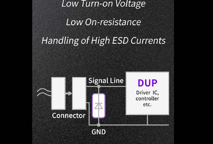
Meets the requirements of low voltage ESD applications when forward biased. When operating under these conditions, they are among the best ESD protection components on the market – with low on-voltage, low on-resistance, and high ESD current handling capabilities.
MOSFET 接地栅极 N 沟道 MOSFET

接地栅极 N 沟道 MOSFET (GGNMOS) 通常用于保护基于 CMOS 的设计免受 ESD 事件的影响。这些器件的结构和操作类似于普通 MOS;但是,它们使用不同的布局技术来优化 ESD 保护器件的性能。
过去,大约 40% 的芯片生产故障与 ESD 有关。虽然可以通过光学显微镜定位故障,但要发现故障并不容易。预防胜于治疗。


