| 自 |
| 浸 |
| 标准作业程序 |
| QFP、QFN |
| BGA LGA |
- 原创内容,请勿转载。
了解芯片封装的历史是了解芯片封装知识的快速方法。
自

说到组件的包装,世界上出现的第一个包装就是 “to”to。组件的晶体不能暴露,它需要
一个保护它的壳,就像我们的内脏不能暴露一样。这就是组件封装的意义所在。
特征 *散热性能好,易于安装散热器(甚至其他主动冷却系统) *适用于各种中等功率电路(电源、放大器、MOSFET 等)的封装 | |
| 类型 | 型 |
| 晶体管型封装 | TO3P、TO92、TO220、TO252、T0263 |
| 金属外壳式包装 | TO3、TO5、TO39、TO46、TO52、TO99、TO100 |
至于 TO 的打包,由于用途不同,衍生出了其他类型的 TO 打包,这里就不多说了,但可以保存截图。
浸

As the first generation of transistors could no longer meet human needs, more complex integrated circuits gradually evolved.
Unable to handle the increasing number of I/O circuits, DIP packaging was also developed. These two long rows of pins are not for nothing. Its main function is to
perform through-hole processes on the PC board. If it's DIP-8, there are 8 pins; if DIP-16, there are 16 pins, and so on. Of course, DIP components come in two-row pin
configurations, but there are also single-row straight-insertion types like SIP and ZIP.
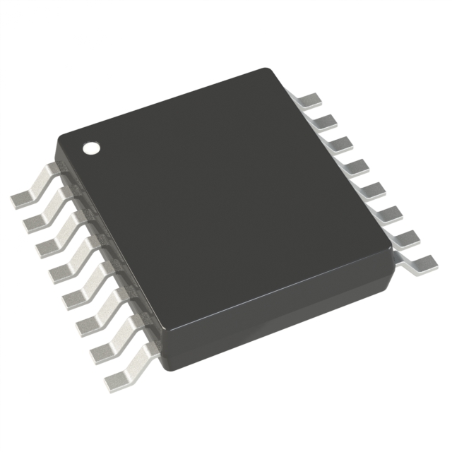
SOP

Highly integrated components still can't meet human needs, so they try to make smaller packages.
By the 1970s, integrated circuits could already integrate 100,000 transistors. High integration, small size, and easy to use. This size was the SOP of that era, and in the world
of SOPs, there were different levels as well. For example, the SOP had a standard shape and surface mount packaging, which was cheaper; TSOP was more advanced with a
thinner and smaller package; VSOP was a micro-sized package; SSOP was an even smaller pin-count package. TSSOP is an even thinner and smaller pin-count package,
essentially the ultimate version of SOP. Of course, there were also even smaller transistor packages for SOTs.
QFP,QFN
If the integrated circuit of SOP is further evolved, it will evolve into QFP and QFN packaging.
Their advantages go beyond high integration and small size. They also offer superior electrical performance and better heat dissipation. It can be said that this is the top-tier
package for integrated circuits to date, suitable only for large-scale or even very large-scale ICs. At the same time, they have a relatively high number of pins. As few as 32
pins and as many as 144 pins are available. Even centipedes can't match it.
BGA LGA

By now, if you think QFP and QFN are top of the line, it's probably because you haven't seen these few packages.
BGA PGA LGA It can be said to further maximize the number of I/O interfaces on a chip. Just looking at its shiny exterior, you know it's no ordinary device. I/O circuit. Its
purpose is to connect external devices; the more, the stronger its functionality.
Most of BGa's pins are in the shape of small particles. A BGA integrated circuit like this can integrate hundreds of beads, or hundreds of pins, which is not comparable to
QFP and SOP.PGA pins are needle-shaped. PGA pins are also located below the chip, but PGA is in the form of needles. LGA is a grid array package.
Its characteristic is that the pin layout design can be carried out according to the number of pins and functional requirements of the chip, that is to say, it can be customized.
Every small chip is a small micro world. It is complicated, just like there are commercial areas, residential areas and industrial areas, which are interlinked. A small mistake will
ruin the whole chip, and the small universe of the whole chip will collapse.And there are countless such small worlds that have been created by humans, and more will be created.