FIRST ORDER
FREE 10% DISCOUNT


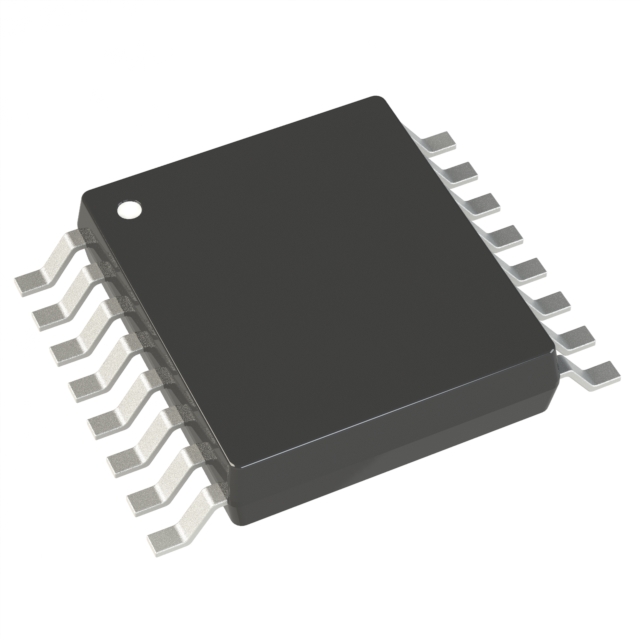
A Comprehensive Guide To AFS090-2QNG180 Fusion® Field Programmable Gate Array (FPGA) IC 60 27648 180-WFQFN Dual Rows, Exposed Pad
Payment and disbursement


Fusion® Field Programmable Gate Array (FPGA) IC 60 27648 180-WFQFN Dual Rows, Exposed Pad
General Description
The Fusion family, based on the highly successful ProASIC®3 and ProASIC3E flash FPGA architecture,has been designed
as a high-performance, programmable, mixed signal platform. By combining anadvanced flash FPGA core with flash
memory blocks and analog peripherals, Fusion devicesdramatically simplify system design and, as a result, dramatically
reduce overall system cost and boardspace.
The state-of-the-art flash memory technology offers high-density integrated flash memory blocks,enabling savings in
cost, power, and board area relative to external flash solutions, while providingincreased flexibility and performance. The
flash memory blocks and integrated analog peripherals enabletrue mixed-mode programmable logic designs. Two
examples are using an on-chip soft processor toimplement a fully functional flash MCU and using high-speed FPGA logic
to offer system and powersupervisory capabilities. Instant On, and capable of operating from a single 3.3 V supply, the
Fusionfamily is ideally suited for system management and control applications.
The devices in the Fusion family are categorized by FPGA core density. Each family member containsmany peripherals,
including flash memory blocks, an analog-to-digital-converter (ADC), high-driveoutputs, both RC and crystal oscillators,
and a real-time counter (RTC). This provides the user with ahigh level of flexibility and integration to support a wide
variety of mixed signal applications. The flashmemory block capacity ranges from 2 Mbits to 8 Mbits. The integrated
12-bit ADC supports up to 30independently configurable input channels.
The on-chip crystal and RC oscillators work in conjunction with the integrated phase-locked loops (PLLs)to provide
clocking support to the FPGA array and on-chip resources. In addition to supporting typicalRTC uses such as watchdog
timer, the Fusion RTC can control the on-chip voltage regulator to powerdown the device (FPGA fabric, flash memory
block, and ADC), enabling a low power standby mode.
The Fusion family offers revolutionary features, never before available in an FPGA. The nonvolatile flashtechnology gives
the Fusion solution the advantage of being a highly secure, low power, single-chipsolution that is Instant On. Fusion is
reprogrammable and offers time-to-market benefits at an ASIC-levelunit cost. These features enable designers to create
high-density systems using existing ASIC or FPGAdesign flows and tools.
Features and Benefits
High-Performance Reprogrammable FlashTechnology
Advanced 130-nm, 7-Layer Metal, Flash-Based CMOSProcess
Nonvolatile, Retains Program when Powered Off
Instant On Single-Chip Solution
350 MHz System Performance
Embedded Flash Memory
User Flash Memory–2 Mbits to 8 Mbits
– Configurable 8-, 16-, or 32-Bit Datapath
– 10 ns Access in Read-Ahead Mode
1 Kbit of Additional FlashROM
Integrated A/D Converter (ADC) and Analog I/O
Up to 12-Bit Resolution and up to 600 Ksps
Internal 2.56 V or External Reference Voltage
ADC: Up to 30 Scalable Analog Input Channels
High-Voltage Input Tolerance: –10.5 V to +12 V
Current Monitor and Temperature Monitor Blocks
Up to 10 MOSFET Gate Driver Outputs
– P- and N-Channel Power MOSFET Support
– Programmable 1, 3, 10, 30 µA, and 20 mA DriveStrengths
ADC Accuracy is Better than 1%
On-Chip Clocking Support
Internal 100 MHz RC Oscillator (accurate to 1%)
Crystal Oscillator Support (32 KHz to 20 MHz)
Programmable Real-Time Counter (RTC)
6 Clock Conditioning Circuits (CCCs) with 1 or 2 Integrated PLLs
– Phase Shift, Multiply/Divide, and Delay Capabilities
– Frequency: Input 1.5–350 MHz, Output 0.75–350 MHz
Low Power Consumption
Single 3.3 V Power Supply with On-Chip 1.5 V Regulator
Sleep and Standby Low-Power Modes
In-System Programming (ISP) and Security
ISP with 128-Bit AES via JTAG
FlashLock® Designed to Protect FPGA Contents
Advanced Digital I/O
1.5 V, 1.8 V, 2.5 V, and 3.3 V Mixed-Voltage Operation
Bank-Selectable I/O Voltages – Up to 5 Banks per Chip
Single-Ended I/O Standards: LVTTL, LVCMOS 3.3V/2.5V/1.8V/1.5V,3.3V PCI/3.3V PCI-X, and LVCMOS 2.5V/5.0 V Input
Differential I/O Standards: LVPECL, LVDS, B-LVDS,M-LVDS
– Built-In I/O Registers
– 700 Mbps DDR Operation
Hot-Swappable I/Os
Programmable Output Slew Rate, Drive Strength, and Weak Pull-Up/Down Resistor
Pin-Compatible Packages across the Fusion® FamilySRAMs and FIFOs
Variable-Aspect-Ratio 4,608-Bit SRAM Blocks (×1, ×2,×4, ×9, and ×18 organizations available)
True Dual-Port SRAM (except ×18)
Programmable Embedded FIFO Control Logic
Soft ARM Cortex-M1 Fusion Devices (M1)
ARM® Cortex-™M1–Enabled
Pigeon Point ATCA IP Support (P1)
Targeted to Pigeon Point® Board ManagementReference (BMR) Starter Kits
Designed in Partnership with Pigeon Point Systems
ARM Cortex-M1 Enabled
MicroBlade Advanced Mezzanine Card Support (U1)
Targeted to Advanced Mezzanine Card (AdvancedMC™Designs)
Designed in Partnership with MicroBlade
8051-Based Module Management Controller (MMC)
How to choose FPGA for your project?
Hot Sales
Pricing And ODER
Stock:
0
Price:
$0
Quantity:
Shipping Cost
$28.63
PostNL International Mail 11-33
?Unconfirmed payment orders may not be able to deliver the normal cancellation of the order, please communicate with the email to confirm before making the relevant payment ~ Attached email phone number The platform has the right to cancel the unconfirmed payment orders do not need to bear the responsibility of default.
Shipment Date
2025/04/18 PM
Delivery Date
5-10 business days
About Logistics:
?Shipping time will be determined according to the logistics time, there will be differences in the place please understand!
| Sub-Total | $0 |
| Shipping: | $28.63 |
| Total | $28.63 |
Please send RFQ , we will respond immediately.
Product:
-
 Afghanistan
-
Afghanistan
-
 Albania
-
 Algeria
-
 American Samoa
-
 Andorra
-
 Angola
-
 Anguilla
-
 Antigua & Barbuda
-
 Argentina
-
 Arizona
-
 Armenia
-
 Aruba
Aruba
-
 Australia
-
 Austria
-
 Azerbaijan
-
 Bahamas
-
 Bahrain
-
 Bangladesh
-
 Barbados
-
 Belarus
-
 Belgium
-
 Belize
-
 Benin
Benin
-
 Bermuda
-
 Bhutan
-
 Bolivia
-
 Bonaire
-
 Bosnia and Herzegovina
-
 Botswana
-
 Brazil
-
 British Virgin Islands
-
 Brunei
-
 Bulgaria
-
 Burkina Faso
-
 Burundi
-
 California
-
 Cambodia
-
 Cameroon
-
 Canada
-
 Cape Verde
-
 Cayman Islands
-
 Central African Republic
-
 Chad
Chad
-
 Chile
Chile
-
 Colombia
-
 Colorado
-
 Congo
Congo
-
 Cook Islands
-
 Costa Rica
-
 Côte d'Ivoire
-
 Croatia
-
 Curaçao
-
 Curacao
-
 Cyprus
-
 Czech Republic
-
 Democratic Republic of Congo
-
Democratic Republic of the Congo
-
 Denmark
-
 Djibouti
-
 Dominica
-
 Dominican Republic
-
 East Timor
-
 Ecuador
-
 Egypt
Egypt
-
 El Salvador
-
 Eritrea
-
 Estonia
-
Eswatini
-
 Ethiopia
-
 Faroe Islands
-
 Fiji
Fiji
-
 Finland
-
 France
-
 French Guiana
-
 French Polynesia
-
 Gabon
Gabon
-
 Gambia
-
 Georgia
-
 Germany
-
 Ghana
Ghana
-
 Gibraltar
-
 Greece
-
 Greenland
-
 Grenada
-
 Guadeloupe
-
 Guam
Guam
-
 Guatemala
-
 Guinea
-
 Guyana
-
 Haiti
Haiti
-
 Honduras
-
 Hong Kong
-
Hong Kong, China
-
 Hungary
-
 Iceland
-
 Idaho
Idaho
-
 India
India
-
 Indonesia
-
 Iraq
Iraq
-
 Ireland
-
 Israel
-
 Italy
Italy
-
Ivory Coast
-
 Jamaica
-
 Japan
Japan
-
 Jordan
-
 Kazakhstan
-
 Kenya
Kenya
-
 Kuwait
-
 Kyrgyzstan
-
 Laos
Laos
-
 Latvia
-
 Lebanon
-
 Lesotho
-
 Liberia
-
 Libya
Libya
-
 Liechtenstein
-
Liechtenstein (Switzerland)
-
 Lithuania
-
 Luxembourg
-
Macao, China
-
 Macau
Macau
-
 Macedonia
-
 Madagascar
-
 Malawi
-
 Malaysia
-
 Maldives
-
 Mali
Mali
-
 Malta
Malta
-
 Marshall Islands
-
 Martinique
-
 Mauritania
-
 Mauritius
-
 Mexico
-
 Micronesia
-
 Moldova
-
 Monaco
-
Monaco (France)
-
 Mongolia
-
 Montenegro
-
 Montserrat
-
 Morocco
-
 Mozambique
-
 Myanmar
-
 Namibia
-
 Nepal
Nepal
-
 Netherlands
-
 Netherlands Antilles
-
 Nevada
-
 New Caledonia
-
 New Zealand
-
 Nicaragua
-
 Niger
Niger
-
 Nigeria
-
North Macedonia
-
 Northern Mariana Islands
-
 Norway
-
 Oman
Oman
-
 Oregon
-
 Other States in US
-
 Pakistan
-
 Palau
Palau
-
Palestinian Authority
-
 Palestinian Territories
-
 Panama
-
 Papua New Guinea
-
 Paraguay
-
 Peru
Peru
-
 Philippines
-
 Poland
-
 Portugal
-
 Puerto Rico
-
 Qatar
Qatar
-
Republic of Moldova
-
Rest of the United States
-
 Réunion
-
Reunion
-
 Romania
-
Rota (Northern Mariana Islands)
-
 Russian
-
Russian Federation
-
 Rwanda
-
Saint Kitts and Nevis
-
 Saint Lucia
-
Saint Maarten (Dutch part)
-
 Saint Martin (French part)
-
 Saint Vincent and the Grenadines
-
Saipan (Northern Mariana Islands)
-
 Samoa
Samoa
-
 San Marino
-
 Saudi Arabia
-
 Senegal
-
 Serbia
-
 Seychelles
-
 Sierra Leone
-
 Singapore
-
 Slovakia
-
 Slovenia
-
Solomon Islands
-
 South Africa
-
 South Korea
-
 Spain
Spain
-
 Sri Lanka
-
 St. Kitts and Nevis
-
 St. Maarten
-
 Suriname
-
 Swaziland (Eswatini)
-
 Sweden
-
 Switzerland
-
 Syria
Syria
-
 Taiwan
-
Taiwan, China
-
 Tajikistan
-
 Tanzania
-
 Thailand
-
Tinian (Northern Mariana Islands)
-
 Togo
Togo
-
 Tonga
Tonga
-
 Trinidad and Tobago
-
 Tunisia
-
 Turkey
-
 Turks and Caicos Islands
-
 Uganda
-
 Ukraine
-
 United Arab Emirates
-
 United Kingdom
-
United Kingdom (Great Britain)
-
 United States
-
 United States Virgin Islands
-
 Uruguay
-
 Utah
Utah
-
 Uzbekistan
-
 Vanuatu
-
 Venezuela
-
 Vietnam
-
 Wallis and Futuna
-
 Washington
-
 Yemen
Yemen
-
 Zambia
-
 Zimbabwe
| Shipping method | Costs | Delivery Time | |
|---|---|---|---|
 SF Express SF Express |
$21.08 | 6-8 business days |


