FIRST ORDER
FREE 10% DISCOUNT


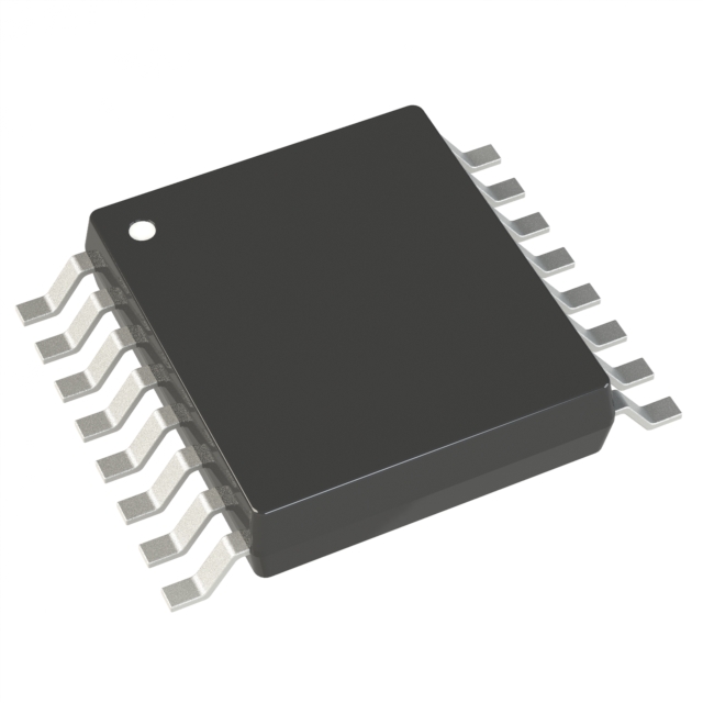
A Comprehensive Guide to EP2C8T144I8N IC FPGA 85 I/O 144TQFP
Payment and disbursement


Cyclone® II Field Programmable Gate Array (FPGA) IC 85 165888 8256 144-LQFP
Introduction
Following the immensely successful first-generation Cyclone® device
family, Altera® Cyclone II FPGAs extend the low-cost FPGA density
range to 68,416 logic elements (LEs) and provide up to 622 usable I/O
pins and up to 1.1 Mbits of embedded memory. Cyclone II FPGAs are
manufactured on 300-mm wafers using TSMC's 90-nm low-k dielectric
process to ensure rapid availability and low cost. By minimizing silicon
area, Cyclone II devices can support complex digital systems on a single
chip at a cost that rivals that of ASICs. Unlike other FPGA vendors who
compromise power consumption and performance for low-cost, Altera’s
latest generation of low-cost FPGAs—Cyclone II FPGAs, offer 60% higher
performance and half the power consumption of competing 90-nm
FPGAs. The low cost and optimized feature set of Cyclone II FPGAs make
them ideal solutions for a wide array of automotive, consumer,
communications, video processing, test and measurement, and other
end-market solutions. Reference designs, system diagrams, and IP, found
at www.altera.com, are available to help you rapidly develop complete
end-market solutions using Cyclone II FPGAs.
Features
The Cyclone II device family offers the following features:
■ High-density architecture with 4,608 to 68,416 LEs
● M4K embedded memory blocks
● Up to 1.1 Mbits of RAM available without reducing available logic
● 4,096 memory bits per block (4,608 bits per block including 512 parity bits)
● Variable port configurations of ×1, ×2, ×4, ×8, ×9, ×16, ×18, ×32, and ×36
● True dual-port (one read and one write, two reads, or two writes) operation for ×1, ×2, ×4, ×8, ×9, ×16, and ×18 modes
● Byte enables for data input masking during writes
● Up to 260-MHz operation
■ Embedded multipliers
● Up to 150 18- × 18-bit multipliers are each configurable as two independent 9- × 9-bit multipliers with up to 250-MHz
performance
● Optional input and output registers
■ Advanced I/O support
● High-speed differential I/O standard support, including LVDS, RSDS, mini-LVDS, LVPECL, differential HSTL, and differential
SSTL
● Single-ended I/O standard support, including 2.5-V and 1.8-V, SSTL class I and II, 1.8-V and 1.5-V HSTL class I and II, 3.3-V PCI
and PCI-X 1.0, 3.3-, 2.5-, 1.8-, and 1.5-V LVCMOS, and 3.3-, 2.5-, and 1.8-V LVTTL
● Peripheral Component Interconnect Special Interest Group (PCI SIG) PCI Local Bus Specification, Revision 3.0 compliance for 3.3-V
operation at 33 or 66 MHz for 32- or 64-bit interfaces
● PCI Express with an external TI PHY and an Altera PCI Express ×1 Megacore® function
● 133-MHz PCI-X 1.0 specification compatibility
● High-speed external memory support, including DDR, DDR2, and SDR SDRAM, and QDRII SRAM supported by drop in
Altera IP MegaCore functions for ease of use
● Three dedicated registers per I/O element (IOE): one input register, one output register, and one output-enable register
● Programmable bus-hold feature
● Programmable output drive strength feature
● Programmable delays from the pin to the IOE or logic array
● I/O bank grouping for unique VCCIO and/or VREF bank settings
● MultiVolt™ I/O standard support for 1.5-, 1.8-, 2.5-, and 3.3-interfaces
● Hot-socketing operation support
● Tri-state with weak pull-up on I/O pins before and during configuration
● Programmable open-drain outputs
● Series on-chip termination support
■ Flexible clock management circuitry
● Hierarchical clock network for up to 402.5-MHz performance
● Up to four PLLs per device provide clock multiplication and division, phase shifting, programmable duty cycle, and external
clock outputs, allowing system-level clock management and skew control
● Up to 16 global clock lines in the global clock network that drive throughout the entire device
■ Device configuration
● Fast serial configuration allows configuration times less than 100 ms
● Decompression feature allows for smaller programming file storage and faster configuration times
● Supports multiple configuration modes: active serial, passive serial, and JTAG-based configuration
● Supports configuration through low-cost serial configuration devices
● Device configuration supports multiple voltages (either 3.3, 2.5, or 1.8 V)
Chip Altera Cyclone naming rules,Chinese chip Will replace it
Hot Sales
Pricing And ODER
Stock:
0
Price:
$52.58
Quantity:
Shipping Cost
$28.63
PostNL International Mail 11-33
?Unconfirmed payment orders may not be able to deliver the normal cancellation of the order, please communicate with the email to confirm before making the relevant payment ~ Attached email phone number The platform has the right to cancel the unconfirmed payment orders do not need to bear the responsibility of default.
Shipment Date
2025/03/29 PM
Delivery Date
5-10 business days
About Logistics:
?Shipping time will be determined according to the logistics time, there will be differences in the place please understand!
| Sub-Total | $52.58 |
| Shipping: | $28.63 |
| Total | $81.21 |
Please send RFQ , we will respond immediately.
Product:
-
 Afghanistan
-
Afghanistan
-
 Albania
-
 Algeria
-
 American Samoa
-
 Andorra
-
 Angola
-
 Anguilla
-
 Antigua & Barbuda
-
 Argentina
-
 Arizona
-
 Armenia
-
 Aruba
Aruba
-
 Australia
-
 Austria
-
 Azerbaijan
-
 Bahamas
-
 Bahrain
-
 Bangladesh
-
 Barbados
-
 Belarus
-
 Belgium
-
 Belize
-
 Benin
Benin
-
 Bermuda
-
 Bhutan
-
 Bolivia
-
 Bonaire
-
 Bosnia and Herzegovina
-
 Botswana
-
 Brazil
-
 British Virgin Islands
-
 Brunei
-
 Bulgaria
-
 Burkina Faso
-
 Burundi
-
 California
-
 Cambodia
-
 Cameroon
-
 Canada
-
 Cape Verde
-
 Cayman Islands
-
 Central African Republic
-
 Chad
Chad
-
 Chile
Chile
-
 Colombia
-
 Colorado
-
 Congo
Congo
-
 Cook Islands
-
 Costa Rica
-
 Côte d'Ivoire
-
 Croatia
-
 Curaçao
-
 Curacao
-
 Cyprus
-
 Czech Republic
-
 Democratic Republic of Congo
-
Democratic Republic of the Congo
-
 Denmark
-
 Djibouti
-
 Dominica
-
 Dominican Republic
-
 East Timor
-
 Ecuador
-
 Egypt
Egypt
-
 El Salvador
-
 Eritrea
-
 Estonia
-
Eswatini
-
 Ethiopia
-
 Faroe Islands
-
 Fiji
Fiji
-
 Finland
-
 France
-
 French Guiana
-
 French Polynesia
-
 Gabon
Gabon
-
 Gambia
-
 Georgia
-
 Germany
-
 Ghana
Ghana
-
 Gibraltar
-
 Greece
-
 Greenland
-
 Grenada
-
 Guadeloupe
-
 Guam
Guam
-
 Guatemala
-
 Guinea
-
 Guyana
-
 Haiti
Haiti
-
 Honduras
-
 Hong Kong
-
Hong Kong, China
-
 Hungary
-
 Iceland
-
 Idaho
Idaho
-
 India
India
-
 Indonesia
-
 Iraq
Iraq
-
 Ireland
-
 Israel
-
 Italy
Italy
-
Ivory Coast
-
 Jamaica
-
 Japan
Japan
-
 Jordan
-
 Kazakhstan
-
 Kenya
Kenya
-
 Kuwait
-
 Kyrgyzstan
-
 Laos
Laos
-
 Latvia
-
 Lebanon
-
 Lesotho
-
 Liberia
-
 Libya
Libya
-
 Liechtenstein
-
Liechtenstein (Switzerland)
-
 Lithuania
-
 Luxembourg
-
Macao, China
-
 Macau
Macau
-
 Macedonia
-
 Madagascar
-
 Malawi
-
 Malaysia
-
 Maldives
-
 Mali
Mali
-
 Malta
Malta
-
 Marshall Islands
-
 Martinique
-
 Mauritania
-
 Mauritius
-
 Mexico
-
 Micronesia
-
 Moldova
-
 Monaco
-
Monaco (France)
-
 Mongolia
-
 Montenegro
-
 Montserrat
-
 Morocco
-
 Mozambique
-
 Myanmar
-
 Namibia
-
 Nepal
Nepal
-
 Netherlands
-
 Netherlands Antilles
-
 Nevada
-
 New Caledonia
-
 New Zealand
-
 Nicaragua
-
 Niger
Niger
-
 Nigeria
-
North Macedonia
-
 Northern Mariana Islands
-
 Norway
-
 Oman
Oman
-
 Oregon
-
 Other States in US
-
 Pakistan
-
 Palau
Palau
-
Palestinian Authority
-
 Palestinian Territories
-
 Panama
-
 Papua New Guinea
-
 Paraguay
-
 Peru
Peru
-
 Philippines
-
 Poland
-
 Portugal
-
 Puerto Rico
-
 Qatar
Qatar
-
Republic of Moldova
-
Rest of the United States
-
 Réunion
-
Reunion
-
 Romania
-
Rota (Northern Mariana Islands)
-
 Russian
-
Russian Federation
-
 Rwanda
-
Saint Kitts and Nevis
-
 Saint Lucia
-
Saint Maarten (Dutch part)
-
 Saint Martin (French part)
-
 Saint Vincent and the Grenadines
-
Saipan (Northern Mariana Islands)
-
 Samoa
Samoa
-
 San Marino
-
 Saudi Arabia
-
 Senegal
-
 Serbia
-
 Seychelles
-
 Sierra Leone
-
 Singapore
-
 Slovakia
-
 Slovenia
-
Solomon Islands
-
 South Africa
-
 South Korea
-
 Spain
Spain
-
 Sri Lanka
-
 St. Kitts and Nevis
-
 St. Maarten
-
 Suriname
-
 Swaziland (Eswatini)
-
 Sweden
-
 Switzerland
-
 Syria
Syria
-
 Taiwan
-
Taiwan, China
-
 Tajikistan
-
 Tanzania
-
 Thailand
-
Tinian (Northern Mariana Islands)
-
 Togo
Togo
-
 Tonga
Tonga
-
 Trinidad and Tobago
-
 Tunisia
-
 Turkey
-
 Turks and Caicos Islands
-
 Uganda
-
 Ukraine
-
 United Arab Emirates
-
 United Kingdom
-
United Kingdom (Great Britain)
-
 United States
-
 United States Virgin Islands
-
 Uruguay
-
 Utah
Utah
-
 Uzbekistan
-
 Vanuatu
-
 Venezuela
-
 Vietnam
-
 Wallis and Futuna
-
 Washington
-
 Yemen
Yemen
-
 Zambia
-
 Zimbabwe
| Shipping method | Costs | Delivery Time | |
|---|---|---|---|
 SF Express SF Express |
$21.08 | 6-8 business days |


