FIRST ORDER
FREE 10% DISCOUNT


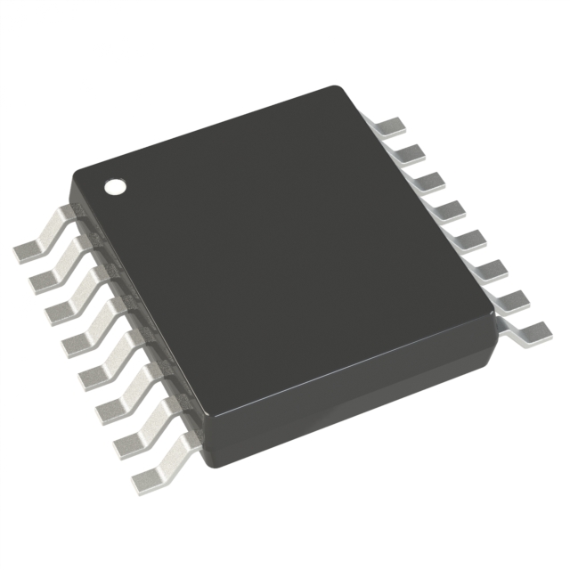
A Comprehensive Guide To ICE5LP1K-SG48ITR iCE40 Ultra™ Field Programmable Gate Array (FPGA) IC 39 65536 1100 48-VFQFN Exposed Pad
Payment and disbursement


iCE40 Ultra™ Field Programmable Gate Array (FPGA) IC 39 65536 1100 48-VFQFN Exposed Pad
General Description
iCE40 Ultra family is an ultra-low power FPGA and sensor manager designed for ultra-low power mobile applications,
such as smartphones, tablets and hand-held devices. The iCE40 Ultra family includes integrated SPI and I²Cblocks to
interface with virtually all mobile sensors and application processors. The iCE40 Ultra family also featurestwo on-chip
oscillators, 10 kHz and 48 MHz. The LFOSC (10 kHz) is ideal for low power function in always-on applications, while
HFOSC (48 MHz) can be used for awaken activities.
The iCE40 Ultra family also features DSP functional block to off-load Application Processor to pre-process information
sent from the mobile sensors. The embedded RGB PWM IP, with the three 24 mA constant current RGB outputs on the
iCE40 Ultra provides all the necessary logic to directly drive the service LED, without the need ofexternal MOSFET or
buffer.
The 500 mA constant current IR driver output provides a direct interface to external LED for application such asIrDA
functions. Users simply implement the modulation logic that meets his needs, and connect the IR driverdirectly to the
LED, without the need of external MOSFET or buffer. This high current IR driver can also be used asBarcode Emulation,
sending barcode information to external Barcode Reader.
The iCE40 Ultra family of devices are targeting for mobile applications to perform functions such as IrDA, ServiceLED,
Barcode Emulation, GPIO Expander, SDIO Level Shift, and other custom functions.
The iCE40 Ultra family features three device densities, from 1100 to 3520 Look Up Tables (LUTs) of logic with
programmable I/Os that can be used as either SPI/I²C interface ports or general purpose I/O’s. It also has up to 80kbits
of Block RAMs to work with user logic.
Features
Flexible Logic Architecture
Three devices with 1100 to 3520 LUTs
Offered in WLCS, ucfBGA and QFN packages
Ultra-low Power Devices
Advanced 40 nm ultra-low power process
As low as 71 µA standby current typical
Embedded Memory
Up to 80 kbits sysMEM™ Embedded Block RAM
Two Hardened I2C Interfaces
Two Hardened SPI Interfaces
Two On-Chip Oscillators
Low Frequency Oscillator – 10 kHz
High Frequency Oscillator – 48 MHz
24 mA Current Drive RGB LED Outputs
Three drive outputs in each device
User selectable sink current up to 24 mA
500 mA Current Drive IR LED Output
One IR drive output in each device
User selectable sink current up to 500 mA
On-chip DSP
Signed and unsigned 8-bit or 16-bit functions
Functions include Multiplier, Accumulator, and Multiply-Accumulate (MAC)
Flexible On-Chip Clocking
Eight low skew global signal resource, six can be directly driven from external pins
One PLL with dynamic interface per device
Flexible Device Configuration
SRAM is configured through:
— Standard SPI Interface
— Internal Nonvolatile Configuration Memory (NVCM)
Ultra-Small Form Factor
As small as 2.078 mm x 2.078 mm
Applications
Smartphones
Tablets and Consumer Handheld Devices
Handheld Commercial and Industrial Devices
Multi Sensor Management Applications
Sensor Pre-processing and Sensor Fusion
Always-On Sensor Applications
USB 3.1 Type C Cable Detect / Power Delivery Applications
How to choose FPGA for your project?
Hot Sales
Pricing And ODER
Stock:
0
Price:
$5
Quantity:
Shipping Cost
$28.63
PostNL International Mail 11-33
?Unconfirmed payment orders may not be able to deliver the normal cancellation of the order, please communicate with the email to confirm before making the relevant payment ~ Attached email phone number The platform has the right to cancel the unconfirmed payment orders do not need to bear the responsibility of default.
Shipment Date
2025/04/23 AM
Delivery Date
5-10 business days
About Logistics:
?Shipping time will be determined according to the logistics time, there will be differences in the place please understand!
| Sub-Total | $5 |
| Shipping: | $28.63 |
| Total | $33.63 |
Please send RFQ , we will respond immediately.
Product:
-
 Afghanistan
-
Afghanistan
-
 Albania
-
 Algeria
-
 American Samoa
-
 Andorra
-
 Angola
-
 Anguilla
-
 Antigua & Barbuda
-
 Argentina
-
 Arizona
-
 Armenia
-
 Aruba
Aruba
-
 Australia
-
 Austria
-
 Azerbaijan
-
 Bahamas
-
 Bahrain
-
 Bangladesh
-
 Barbados
-
 Belarus
-
 Belgium
-
 Belize
-
 Benin
Benin
-
 Bermuda
-
 Bhutan
-
 Bolivia
-
 Bonaire
-
 Bosnia and Herzegovina
-
 Botswana
-
 Brazil
-
 British Virgin Islands
-
 Brunei
-
 Bulgaria
-
 Burkina Faso
-
 Burundi
-
 California
-
 Cambodia
-
 Cameroon
-
 Canada
-
 Cape Verde
-
 Cayman Islands
-
 Central African Republic
-
 Chad
Chad
-
 Chile
Chile
-
 Colombia
-
 Colorado
-
 Congo
Congo
-
 Cook Islands
-
 Costa Rica
-
 Côte d'Ivoire
-
 Croatia
-
 Curaçao
-
 Curacao
-
 Cyprus
-
 Czech Republic
-
 Democratic Republic of Congo
-
Democratic Republic of the Congo
-
 Denmark
-
 Djibouti
-
 Dominica
-
 Dominican Republic
-
 East Timor
-
 Ecuador
-
 Egypt
Egypt
-
 El Salvador
-
 Eritrea
-
 Estonia
-
Eswatini
-
 Ethiopia
-
 Faroe Islands
-
 Fiji
Fiji
-
 Finland
-
 France
-
 French Guiana
-
 French Polynesia
-
 Gabon
Gabon
-
 Gambia
-
 Georgia
-
 Germany
-
 Ghana
Ghana
-
 Gibraltar
-
 Greece
-
 Greenland
-
 Grenada
-
 Guadeloupe
-
 Guam
Guam
-
 Guatemala
-
 Guinea
-
 Guyana
-
 Haiti
Haiti
-
 Honduras
-
 Hong Kong
-
Hong Kong, China
-
 Hungary
-
 Iceland
-
 Idaho
Idaho
-
 India
India
-
 Indonesia
-
 Iraq
Iraq
-
 Ireland
-
 Israel
-
 Italy
Italy
-
Ivory Coast
-
 Jamaica
-
 Japan
Japan
-
 Jordan
-
 Kazakhstan
-
 Kenya
Kenya
-
 Kuwait
-
 Kyrgyzstan
-
 Laos
Laos
-
 Latvia
-
 Lebanon
-
 Lesotho
-
 Liberia
-
 Libya
Libya
-
 Liechtenstein
-
Liechtenstein (Switzerland)
-
 Lithuania
-
 Luxembourg
-
Macao, China
-
 Macau
Macau
-
 Macedonia
-
 Madagascar
-
 Malawi
-
 Malaysia
-
 Maldives
-
 Mali
Mali
-
 Malta
Malta
-
 Marshall Islands
-
 Martinique
-
 Mauritania
-
 Mauritius
-
 Mexico
-
 Micronesia
-
 Moldova
-
 Monaco
-
Monaco (France)
-
 Mongolia
-
 Montenegro
-
 Montserrat
-
 Morocco
-
 Mozambique
-
 Myanmar
-
 Namibia
-
 Nepal
Nepal
-
 Netherlands
-
 Netherlands Antilles
-
 Nevada
-
 New Caledonia
-
 New Zealand
-
 Nicaragua
-
 Niger
Niger
-
 Nigeria
-
North Macedonia
-
 Northern Mariana Islands
-
 Norway
-
 Oman
Oman
-
 Oregon
-
 Other States in US
-
 Pakistan
-
 Palau
Palau
-
Palestinian Authority
-
 Palestinian Territories
-
 Panama
-
 Papua New Guinea
-
 Paraguay
-
 Peru
Peru
-
 Philippines
-
 Poland
-
 Portugal
-
 Puerto Rico
-
 Qatar
Qatar
-
Republic of Moldova
-
Rest of the United States
-
 Réunion
-
Reunion
-
 Romania
-
Rota (Northern Mariana Islands)
-
 Russian
-
Russian Federation
-
 Rwanda
-
Saint Kitts and Nevis
-
 Saint Lucia
-
Saint Maarten (Dutch part)
-
 Saint Martin (French part)
-
 Saint Vincent and the Grenadines
-
Saipan (Northern Mariana Islands)
-
 Samoa
Samoa
-
 San Marino
-
 Saudi Arabia
-
 Senegal
-
 Serbia
-
 Seychelles
-
 Sierra Leone
-
 Singapore
-
 Slovakia
-
 Slovenia
-
Solomon Islands
-
 South Africa
-
 South Korea
-
 Spain
Spain
-
 Sri Lanka
-
 St. Kitts and Nevis
-
 St. Maarten
-
 Suriname
-
 Swaziland (Eswatini)
-
 Sweden
-
 Switzerland
-
 Syria
Syria
-
 Taiwan
-
Taiwan, China
-
 Tajikistan
-
 Tanzania
-
 Thailand
-
Tinian (Northern Mariana Islands)
-
 Togo
Togo
-
 Tonga
Tonga
-
 Trinidad and Tobago
-
 Tunisia
-
 Turkey
-
 Turks and Caicos Islands
-
 Uganda
-
 Ukraine
-
 United Arab Emirates
-
 United Kingdom
-
United Kingdom (Great Britain)
-
 United States
-
 United States Virgin Islands
-
 Uruguay
-
 Utah
Utah
-
 Uzbekistan
-
 Vanuatu
-
 Venezuela
-
 Vietnam
-
 Wallis and Futuna
-
 Washington
-
 Yemen
Yemen
-
 Zambia
-
 Zimbabwe
| Shipping method | Costs | Delivery Time | |
|---|---|---|---|
 SF Express SF Express |
$21.08 | 6-8 business days |


