FIRST ORDER
FREE 10% DISCOUNT


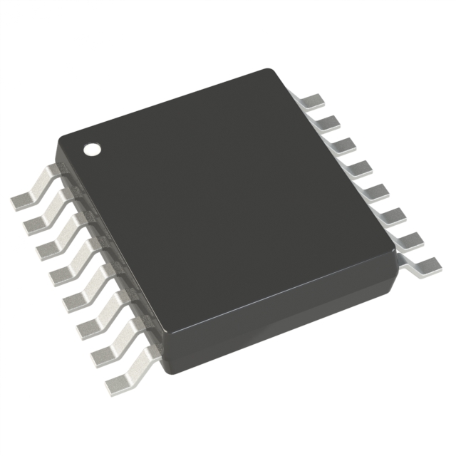
A Comprehensive Guide To LIFCL-40-7MG121I CrossLink-NX™ Field Programmable Gate Array (FPGA) IC 72 1548288 39000 121-VFBGA, CSPBGA
Payment and disbursement


CrossLink-NX™ Field Programmable Gate Array (FPGA) IC 72 1548288 39000 121-VFBGA, CSPBGA
General Description
CrossLink™-NX family of low-power FPGAs can be used in a wide range of applications, and are optimized for bridging and
processing needs in Embedded Vision applications – supporting a variety of high bandwidth sensor and display interfaces,
video processing and machine learning inferencing. It is built on Lattice Nexus FPGA platform, using low-power 28 nm
FD-SOI technology. It combines the extreme flexibility of an FPGA with the low power and high reliability (due to extremely
low SER) of FD-SOI technology, and offers small footprint package options.
CrossLink-NX supports a variety of interfaces including MIPI D-PHY (CSI-2, DSI), LVDS, SLVS, subLVDS, PCI Express (Gen1,
Gen2), SGMII (Gigabit Ethernet), and more.
Processing features of CrossLink-NX include up to 39K Logic Cells, 56 18x18 multipliers, 2.9 Mb of embedded memory
(consisting of EBR and LRAM blocks), distributed memory, DRAM interfaces (supporting DDR3, DDR3L, LPDDR2, and
LPDDR3 up to 1066 Mbps x16 data width).
CrossLink-NX FPGAs support fast configuration of its reconfigurable SRAM-based logic fabric, and ultra-fast configuration
(in under 3 ms) of its programmable sysI/O™. Security features to secure user designs include bitstream encryption and
password protection. In addition to the high reliability inherent to FD-SOI technology (due to its extremely low SER), active
reliability features such as built-in frame-based SED/SEC (for SRAM-based logic fabric), and ECC (for EBR and LRAM) are
also supported. Built-in ADC is available in each device for system monitoring functions.
Lattice Radiant™ design software allows large complex user designs to be efficiently implemented on CrossLink-NX FPGA
family. Synthesis library support for CrossLink-NX devices is available for popular logic synthesis tools. Radiant tools use the
synthesis tool output along with constraints from its floor planning tools, to place and route the user design in
CrossLink-NX device. The tools extract timing from the routing, and back-annotate it into the design for timing verification.
Lattice provides many pre-engineered IP (Intellectual Property) modules for CrossLink-NX family. By using these
configurable soft IP cores as standardized blocks, you are free to concentrate on the unique aspects of your design,
increasing your productivity.
Features
Programmable Architecture
17K to 39K logic cells
24 to 56 18 x 18 multipliers (in sysDSP™ blocks)
2.5 to 2.9 Mb of embedded memory blocks (EBR, LRAM)
36 to 192 programmable sysI/O (High Performance and Wide Range I/O)
MIPI D-PHY
Up to two hardened 4-lane MIPI D-PHY interfaces
Up to eight lanes total
Transmit or receive
Supports CSI-2, DSI
20 Gbps aggregate bandwidth
2.5 Gbps per lane, 10 Gbps per D-PHY interface
Additional Soft D-PHY interfaces supported by High Performance (HP) sysI/O
Transmit or receive
Supports CSI-2, DSI
Up to 1.5 Gbps per lane
Programmable sysI/O supports wide variety of interfaces
High Performance (HP) on bottom I/O dual rank
Supports up to 1.8 V VCCIO
Mixed voltage support (1.0 V, 1.2 V, 1.5 V, 1.8 V)
High-speed differential up to 1.5 Gbps
Supports soft D-PHY (Tx/Rx), LVDS 7:1 (Tx/Rx), SLVS (Tx/Rx), subLVDS (Rx)
Supports SGMII (Gb Ethernet) – 2 channels (Tx/Rx) at 1.25 Gbps
Dedicated DDR3/DDR3L and LPDDR2/LPDDR3 memory support with DQS logic, up to 1066 Mbps data-rate and
x16 data-width
Wide Range (WR) on Left, Right and Top I/O Banks
Supports up to 3.3 V VCCIO
Mixed voltage support (1.2 V, 1.5 V, 1.8 V, 2.5 V, 3.3 V)
Programmable slew rate (slow, med, fast)
Controlled impedance mode
Emulated LVDS support
Hot-socketing
Power Modes – Low Power versus High Performance
User selectable
Low-Power mode for power and/or thermal challenges
High-Performance mode for faster processing
Small footprint package options
4 x 4 mm2to 10 x 10 mm2 package options
2x SGMII CDR at up to 1.25 Gbps – to support 2 channels SGMII using HP I/O
CDR for RX
8b/10b decoding
Independent Loss of Lock (LOL) detector for each CDR block
sysCLOCK™ analog PLLs
Three in 39K LC and two in 17K LC device
Six outputs per PLL
Fractional N
Programmable and dynamic phase control
sysDSP Enhanced DSP blocks
Hardened pre-adder
Dynamic Shift for AI/ML support
Four 18 x 18, eight 9 x 9, two 18 x 36, or 36 x 36
Advanced 18 x 36, two 18 x 18, or four 8 x 8 MAC
Flexible memory resources
Up to 1.5 Mb sysMEM™ Embedded Block RAM EBR)
Programmable width
ECC
FIFO
80k to 240k bits distributed RAM
Large RAM Blocks
0.5 Mbits per block
Up to five blocks (2.5 Mb total) per device
SERDES – PCIe Gen2 x1 channel (Tx/Rx) hard IP in 39K LC device
Hard IP supports
Gen1, Gen2, Multi-Function, End Point, Root Complex
APB control bus
AHB-Lite for data bus
Internal bus interface support
APB control bus
AHB-Lite for data bus
AXI4-streaming
Configuration – Fast, Secure
SPI – x1, x2, x4 up to 150 MHz
Master and Slave SPI support
JTAG
I²C and I3C
Ultrafast I/O configuration for instant-on support
Less than 15 ms full device configuration for LIFCL-40
Bitstream Security
Encryption
Cryptographic engine
Bitstream encryption – using AES-256
Bitstream authentication – using ECDSA
Hashing algorithms – SHA, HMAC
True Random Number Generator
AES 128/256 Encryption
Single Event Upset (SEU) Mitigation Support
Extremely low Soft Error Rate (SER) due to FD SOI technology
Soft Error Detect – Embedded hard macro
Soft Error Correction – Without stopping user operation
Soft Error Injection – Emulate SEU event to debug system error handling
ADC – 1 MSPS, 12-bit SAR
2 ADCs per device
3 Continuous-time Comparators
Simultaneous sampling
System Level Support
IEEE 1149.1 and IEEE 1532 compliant
Reveal Logic Analyzer
On-chip oscillator for initialization and general use
1.0 V core power supply
How to choose FPGA for your project?
Hot Sales
Pricing And ODER
Stock:
0
Price:
$43.23
Quantity:
Shipping Cost
$28.63
PostNL International Mail 11-33
?Unconfirmed payment orders may not be able to deliver the normal cancellation of the order, please communicate with the email to confirm before making the relevant payment ~ Attached email phone number The platform has the right to cancel the unconfirmed payment orders do not need to bear the responsibility of default.
Shipment Date
2025/04/30 PM
Delivery Date
5-10 business days
About Logistics:
?Shipping time will be determined according to the logistics time, there will be differences in the place please understand!
| Sub-Total | $43.23 |
| Shipping: | $28.63 |
| Total | $71.86 |
Please send RFQ , we will respond immediately.
Product:
-
 Afghanistan
-
Afghanistan
-
 Albania
-
 Algeria
-
 American Samoa
-
 Andorra
-
 Angola
-
 Anguilla
-
 Antigua & Barbuda
-
 Argentina
-
 Arizona
-
 Armenia
-
 Aruba
Aruba
-
 Australia
-
 Austria
-
 Azerbaijan
-
 Bahamas
-
 Bahrain
-
 Bangladesh
-
 Barbados
-
 Belarus
-
 Belgium
-
 Belize
-
 Benin
Benin
-
 Bermuda
-
 Bhutan
-
 Bolivia
-
 Bonaire
-
 Bosnia and Herzegovina
-
 Botswana
-
 Brazil
-
 British Virgin Islands
-
 Brunei
-
 Bulgaria
-
 Burkina Faso
-
 Burundi
-
 California
-
 Cambodia
-
 Cameroon
-
 Canada
-
 Cape Verde
-
 Cayman Islands
-
 Central African Republic
-
 Chad
Chad
-
 Chile
Chile
-
 Colombia
-
 Colorado
-
 Congo
Congo
-
 Cook Islands
-
 Costa Rica
-
 Côte d'Ivoire
-
 Croatia
-
 Curaçao
-
 Curacao
-
 Cyprus
-
 Czech Republic
-
 Democratic Republic of Congo
-
Democratic Republic of the Congo
-
 Denmark
-
 Djibouti
-
 Dominica
-
 Dominican Republic
-
 East Timor
-
 Ecuador
-
 Egypt
Egypt
-
 El Salvador
-
 Eritrea
-
 Estonia
-
Eswatini
-
 Ethiopia
-
 Faroe Islands
-
 Fiji
Fiji
-
 Finland
-
 France
-
 French Guiana
-
 French Polynesia
-
 Gabon
Gabon
-
 Gambia
-
 Georgia
-
 Germany
-
 Ghana
Ghana
-
 Gibraltar
-
 Greece
-
 Greenland
-
 Grenada
-
 Guadeloupe
-
 Guam
Guam
-
 Guatemala
-
 Guinea
-
 Guyana
-
 Haiti
Haiti
-
 Honduras
-
 Hong Kong
-
Hong Kong, China
-
 Hungary
-
 Iceland
-
 Idaho
Idaho
-
 India
India
-
 Indonesia
-
 Iraq
Iraq
-
 Ireland
-
 Israel
-
 Italy
Italy
-
Ivory Coast
-
 Jamaica
-
 Japan
Japan
-
 Jordan
-
 Kazakhstan
-
 Kenya
Kenya
-
 Kuwait
-
 Kyrgyzstan
-
 Laos
Laos
-
 Latvia
-
 Lebanon
-
 Lesotho
-
 Liberia
-
 Libya
Libya
-
 Liechtenstein
-
Liechtenstein (Switzerland)
-
 Lithuania
-
 Luxembourg
-
Macao, China
-
 Macau
Macau
-
 Macedonia
-
 Madagascar
-
 Malawi
-
 Malaysia
-
 Maldives
-
 Mali
Mali
-
 Malta
Malta
-
 Marshall Islands
-
 Martinique
-
 Mauritania
-
 Mauritius
-
 Mexico
-
 Micronesia
-
 Moldova
-
 Monaco
-
Monaco (France)
-
 Mongolia
-
 Montenegro
-
 Montserrat
-
 Morocco
-
 Mozambique
-
 Myanmar
-
 Namibia
-
 Nepal
Nepal
-
 Netherlands
-
 Netherlands Antilles
-
 Nevada
-
 New Caledonia
-
 New Zealand
-
 Nicaragua
-
 Niger
Niger
-
 Nigeria
-
North Macedonia
-
 Northern Mariana Islands
-
 Norway
-
 Oman
Oman
-
 Oregon
-
 Other States in US
-
 Pakistan
-
 Palau
Palau
-
Palestinian Authority
-
 Palestinian Territories
-
 Panama
-
 Papua New Guinea
-
 Paraguay
-
 Peru
Peru
-
 Philippines
-
 Poland
-
 Portugal
-
 Puerto Rico
-
 Qatar
Qatar
-
Republic of Moldova
-
Rest of the United States
-
 Réunion
-
Reunion
-
 Romania
-
Rota (Northern Mariana Islands)
-
 Russian
-
Russian Federation
-
 Rwanda
-
Saint Kitts and Nevis
-
 Saint Lucia
-
Saint Maarten (Dutch part)
-
 Saint Martin (French part)
-
 Saint Vincent and the Grenadines
-
Saipan (Northern Mariana Islands)
-
 Samoa
Samoa
-
 San Marino
-
 Saudi Arabia
-
 Senegal
-
 Serbia
-
 Seychelles
-
 Sierra Leone
-
 Singapore
-
 Slovakia
-
 Slovenia
-
Solomon Islands
-
 South Africa
-
 South Korea
-
 Spain
Spain
-
 Sri Lanka
-
 St. Kitts and Nevis
-
 St. Maarten
-
 Suriname
-
 Swaziland (Eswatini)
-
 Sweden
-
 Switzerland
-
 Syria
Syria
-
 Taiwan
-
Taiwan, China
-
 Tajikistan
-
 Tanzania
-
 Thailand
-
Tinian (Northern Mariana Islands)
-
 Togo
Togo
-
 Tonga
Tonga
-
 Trinidad and Tobago
-
 Tunisia
-
 Turkey
-
 Turks and Caicos Islands
-
 Uganda
-
 Ukraine
-
 United Arab Emirates
-
 United Kingdom
-
United Kingdom (Great Britain)
-
 United States
-
 United States Virgin Islands
-
 Uruguay
-
 Utah
Utah
-
 Uzbekistan
-
 Vanuatu
-
 Venezuela
-
 Vietnam
-
 Wallis and Futuna
-
 Washington
-
 Yemen
Yemen
-
 Zambia
-
 Zimbabwe
| Shipping method | Costs | Delivery Time | |
|---|---|---|---|
 SF Express SF Express |
$21.08 | 6-8 business days |


