FIRST ORDER
FREE 10% DISCOUNT


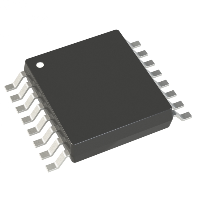
A Comprehensive Guide To MC9S12DG256MPVE Microcontroller IC 16-Bit 25MHz 256KB (256K x 8) FLASH 112-LQFP (20x20)
Payment and disbursement


HCS12 HCS12 Microcontroller IC 16-Bit 25MHz 256KB (256K x 8) FLASH 112-LQFP (20x20)
16-Bit Microcontroller
Designed for automotive multiplexing applications, members of the MC9S12D-Family of 16 bit Flashbased
microcontrollers are fully pin compatible and enable users to choose between different memory
and peripheral options for scalable designs. All MC9S12D-Family members are composed of standard
on-chip peripherals including a 16-bit central processing unit (CPU12), up to 512K bytes of Flash
EEPROM, 14K bytes of RAM, 4K bytes of EEPROM, two asynchronous serial communications
interfaces (SCI), three serial peripheral interfaces (SPI), IIC-bus, an enhanced capture timer (ECT), two
8-channel 10-bit analog-to-digital converters (ADC), an eight-channel pulse-width modulator (PWM),
J1850 interface and up to five CAN 2.0 A, B software compatible modules (MSCAN12). System
resource mapping, clock generation, interrupt control and bus interfacing are managed by the system
integration module (SIM). The MC9S12D-Family has full 16-bit data paths throughout, however, the
external bus can operate in an 8-bit narrow mode so single 8-bit wide memory can be interfaced for
lower cost systems. The inclusion of a PLL circuit allows power consumption and performance to be
adjusted to suit operational requirements. In addition to the I/O ports available in each module, up to 22
I/O ports are available with interrupt capability allowing Wake-Up from STOP or WAIT mode.
Features
• 16-bit CPU12
— Upward compatible with M68HC11 instruction set
— Interrupt stacking and programmer’s model identical to M68HC11
— HCS12 Instruction queue
— Enhanced indexed addressing
• Multiplexed bus
— Single chip or expanded
— 16 address/16 data wide or 16 address/8 data narrow modes
— External address space 1MByte for Data and Program space (112 pin package only)
• Wake-up interrupt inputs depending on the package option
— 8-bit port H
— 2-bit port J1:0
— 2-bit port J7:6 shared with IIC, CAN4 and CAN0 module
— 8-bit port P shared with PWM or SPI1,2
• Memory options
— 32K, 64K, 128K, 256K, 512K Byte Flash EEPROM
— 1K, 2K, 4K Byte EEPROM
— 2K, 4K, 8K, 12K, 14K Byte RAM
• Analog-to-Digital Converters
— One or two 8-channel modules with 10-bit resolution depending on the package option
— External conversion trigger capability
• Up to five 1M bit per second, CAN 2.0 A, B software compatible modules
— Five receive and three transmit buffers
— Flexible identifier filter programmable as 2 x 32 bit, 4 x 16 bit or 8 x 8 bit
— Four separate interrupt channels for Receive, Transmit, Error and Wake-up
— Low-pass filter wake-up function in STOP mode
— Loop-back for self test operation
• Enhanced Capture Timer (ECT)
— 16-bit main counter with 7-bit prescaler
— 8 programmable input capture or output compare channels; 4 of the 8 input captures with buffer
— Input capture filters and buffers, three successive captures on four channels, or two captures on four
channels with a capture/compare selectable on the remaining four
— Four 8-bit or two 16-bit pulse accumulators
— 16-bit modulus down-counter with 4-bit prescaler
— Four user-selectable delay counters for signal filtering
• 8 PWM channels with programmable period and duty cycle (7 channels on 80 Pin Packages)
— 8-bit, 8-channel or 16-bit, 4-channel
— Separate control for each pulse width and duty cycle
— Center- or left-aligned outputs
— Programmable clock select logic with a wide range of frequencies
• Serial interfaces
— Two asynchronous serial communications interfaces (SCI)
— Up to three synchronous serial peripheral interfaces (SPI)
— IIC
• SAE J1850 Compatible Module (BDLC)
— 10.4 kbps Variable Pulse Width format
— Byte level receive and transmit
— 4x receive mode supported
• SIM (System Integration Module)
— CRG (windowed COP watchdog, real time interrupt, clock monitor, clock generation and reset)
— MEBI (multiplexed external bus interface)
— INT (interrupt control)
• Clock generation
— Phase-locked loop clock frequency multiplier
— Limp home mode in absence of external clock
— Clock Monitor
— Low power 0.5 to 16 MHz crystal oscillator reference clock
• Operating frequency for ambient temperatures TA -40°C <= TA <= 125°C
— 50MHz equivalent to 25MHz Bus Speed for single chip
40MHz equivalent to 20MHz Bus Speed in expanded bus modes.
• Internal 5V to 2.5V Regulator
• 112-Pin LQFP or 80-Pin QFP package
— I/O lines with 5V input and drive capability
— 5V A/D converter inputs and 5V I/O
— 2.5V logic supply
• Development support
— Single-wire background debug™ mode (BDM)
— On-chip hardware breakpoints
NXP Electronics components unboxing,humidity card changed color chip can used?
Hot Sales
Pricing And ODER
Stock:
0
Price:
$0
Quantity:
Shipping Cost
$28.63
PostNL International Mail 11-33
?Unconfirmed payment orders may not be able to deliver the normal cancellation of the order, please communicate with the email to confirm before making the relevant payment ~ Attached email phone number The platform has the right to cancel the unconfirmed payment orders do not need to bear the responsibility of default.
Shipment Date
2025/04/23 AM
Delivery Date
5-10 business days
About Logistics:
?Shipping time will be determined according to the logistics time, there will be differences in the place please understand!
| Sub-Total | $0 |
| Shipping: | $28.63 |
| Total | $28.63 |
Please send RFQ , we will respond immediately.
Product:
-
 Afghanistan
-
Afghanistan
-
 Albania
-
 Algeria
-
 American Samoa
-
 Andorra
-
 Angola
-
 Anguilla
-
 Antigua & Barbuda
-
 Argentina
-
 Arizona
-
 Armenia
-
 Aruba
Aruba
-
 Australia
-
 Austria
-
 Azerbaijan
-
 Bahamas
-
 Bahrain
-
 Bangladesh
-
 Barbados
-
 Belarus
-
 Belgium
-
 Belize
-
 Benin
Benin
-
 Bermuda
-
 Bhutan
-
 Bolivia
-
 Bonaire
-
 Bosnia and Herzegovina
-
 Botswana
-
 Brazil
-
 British Virgin Islands
-
 Brunei
-
 Bulgaria
-
 Burkina Faso
-
 Burundi
-
 California
-
 Cambodia
-
 Cameroon
-
 Canada
-
 Cape Verde
-
 Cayman Islands
-
 Central African Republic
-
 Chad
Chad
-
 Chile
Chile
-
 Colombia
-
 Colorado
-
 Congo
Congo
-
 Cook Islands
-
 Costa Rica
-
 Côte d'Ivoire
-
 Croatia
-
 Curaçao
-
 Curacao
-
 Cyprus
-
 Czech Republic
-
 Democratic Republic of Congo
-
Democratic Republic of the Congo
-
 Denmark
-
 Djibouti
-
 Dominica
-
 Dominican Republic
-
 East Timor
-
 Ecuador
-
 Egypt
Egypt
-
 El Salvador
-
 Eritrea
-
 Estonia
-
Eswatini
-
 Ethiopia
-
 Faroe Islands
-
 Fiji
Fiji
-
 Finland
-
 France
-
 French Guiana
-
 French Polynesia
-
 Gabon
Gabon
-
 Gambia
-
 Georgia
-
 Germany
-
 Ghana
Ghana
-
 Gibraltar
-
 Greece
-
 Greenland
-
 Grenada
-
 Guadeloupe
-
 Guam
Guam
-
 Guatemala
-
 Guinea
-
 Guyana
-
 Haiti
Haiti
-
 Honduras
-
 Hong Kong
-
Hong Kong, China
-
 Hungary
-
 Iceland
-
 Idaho
Idaho
-
 India
India
-
 Indonesia
-
 Iraq
Iraq
-
 Ireland
-
 Israel
-
 Italy
Italy
-
Ivory Coast
-
 Jamaica
-
 Japan
Japan
-
 Jordan
-
 Kazakhstan
-
 Kenya
Kenya
-
 Kuwait
-
 Kyrgyzstan
-
 Laos
Laos
-
 Latvia
-
 Lebanon
-
 Lesotho
-
 Liberia
-
 Libya
Libya
-
 Liechtenstein
-
Liechtenstein (Switzerland)
-
 Lithuania
-
 Luxembourg
-
Macao, China
-
 Macau
Macau
-
 Macedonia
-
 Madagascar
-
 Malawi
-
 Malaysia
-
 Maldives
-
 Mali
Mali
-
 Malta
Malta
-
 Marshall Islands
-
 Martinique
-
 Mauritania
-
 Mauritius
-
 Mexico
-
 Micronesia
-
 Moldova
-
 Monaco
-
Monaco (France)
-
 Mongolia
-
 Montenegro
-
 Montserrat
-
 Morocco
-
 Mozambique
-
 Myanmar
-
 Namibia
-
 Nepal
Nepal
-
 Netherlands
-
 Netherlands Antilles
-
 Nevada
-
 New Caledonia
-
 New Zealand
-
 Nicaragua
-
 Niger
Niger
-
 Nigeria
-
North Macedonia
-
 Northern Mariana Islands
-
 Norway
-
 Oman
Oman
-
 Oregon
-
 Other States in US
-
 Pakistan
-
 Palau
Palau
-
Palestinian Authority
-
 Palestinian Territories
-
 Panama
-
 Papua New Guinea
-
 Paraguay
-
 Peru
Peru
-
 Philippines
-
 Poland
-
 Portugal
-
 Puerto Rico
-
 Qatar
Qatar
-
Republic of Moldova
-
Rest of the United States
-
 Réunion
-
Reunion
-
 Romania
-
Rota (Northern Mariana Islands)
-
 Russian
-
Russian Federation
-
 Rwanda
-
Saint Kitts and Nevis
-
 Saint Lucia
-
Saint Maarten (Dutch part)
-
 Saint Martin (French part)
-
 Saint Vincent and the Grenadines
-
Saipan (Northern Mariana Islands)
-
 Samoa
Samoa
-
 San Marino
-
 Saudi Arabia
-
 Senegal
-
 Serbia
-
 Seychelles
-
 Sierra Leone
-
 Singapore
-
 Slovakia
-
 Slovenia
-
Solomon Islands
-
 South Africa
-
 South Korea
-
 Spain
Spain
-
 Sri Lanka
-
 St. Kitts and Nevis
-
 St. Maarten
-
 Suriname
-
 Swaziland (Eswatini)
-
 Sweden
-
 Switzerland
-
 Syria
Syria
-
 Taiwan
-
Taiwan, China
-
 Tajikistan
-
 Tanzania
-
 Thailand
-
Tinian (Northern Mariana Islands)
-
 Togo
Togo
-
 Tonga
Tonga
-
 Trinidad and Tobago
-
 Tunisia
-
 Turkey
-
 Turks and Caicos Islands
-
 Uganda
-
 Ukraine
-
 United Arab Emirates
-
 United Kingdom
-
United Kingdom (Great Britain)
-
 United States
-
 United States Virgin Islands
-
 Uruguay
-
 Utah
Utah
-
 Uzbekistan
-
 Vanuatu
-
 Venezuela
-
 Vietnam
-
 Wallis and Futuna
-
 Washington
-
 Yemen
Yemen
-
 Zambia
-
 Zimbabwe
| Shipping method | Costs | Delivery Time | |
|---|---|---|---|
 SF Express SF Express |
$21.08 | 6-8 business days |


