FIRST ORDER
FREE 10% DISCOUNT


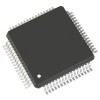
A Comprehensive Guide To MC9S12XET256MAA Microcontroller IC 16-Bit 50MHz 256KB (256K x 8) FLASH 80-QFP (14x14)
Payment and disbursement


HCS12X HCS12X Microcontroller IC 16-Bit 50MHz 256KB (256K x 8) FLASH 80-QFP (14x14)
MC9S12XEP100
Covers MC9S12XE Family
Introduction
The MC9S12XE-Family of micro controllers is a further development of the S12XD-Family including
new features for enhanced system integrity and greater functionality. These new features include a
Memory Protection Unit (MPU) and Error Correction Code (ECC) on the Flash memory together with
enhanced EEPROM functionality (EEE), an enhanced XGATE, an Internally filtered, frequency
modulated Phase Locked Loop (IPLL) and an enhanced ATD. The E-Family extends the S12X product
range up to 1MB of Flash memory with increased I/O capability in the 208-pin version of the flagship
MC9S12XE100.
The MC9S12XE-Family delivers 32-bit performance with all the advantages and efficiencies of a 16 bit
MCU. It retains the low cost, power consumption, EMC and code-size efficiency advantages currently
enjoyed by users of Freescale’s existing 16-Bit MC9S12 and S12X MCU families. There is a high level of
compatibility between the S12XE and S12XD families.
The MC9S12XE-Family features an enhanced version of the performance-boosting XGATE co-processor
which is programmable in “C” language and runs at twice the bus frequency of the S12X with an
instruction set optimized for data movement, logic and bit manipulation instructions and which can service
any peripheral module on the device. The new enhanced version has improved interrupt handling
capability and is fully compatible with the existing XGATE module.
The MC9S12XE-Family is composed of standard on-chip peripherals including up to 64Kbytes of RAM,
eight asynchronous serial communications interfaces (SCI), three serial peripheral interfaces (SPI), an 8-
channel IC/OC enhanced capture timer (ECT), two 16-channel, 12-bit analog-to-digital converters, an 8-
channel pulse-width modulator (PWM), five CAN 2.0 A, B software compatible modules (MSCAN12),
two inter-IC bus blocks (IIC), an 8-channel 24-bit periodic interrupt timer (PIT) and an 8-channel 16-bit
standard timer module (TIM).
The MC9S12XE-Family uses 16-bit wide accesses without wait states for all peripherals and memories.
The non-multiplexed expanded bus interface available on the 144/208-Pin versions allows an easy
interface to external memories.
In addition to the I/O ports available in each module, up to 26 further I/O ports are available with interrupt
capability allowing Wake-Up from STOP or WAIT modes. The MC9S12XE-Family is available in 208-
Pin MAPBGA, 144-Pin LQFP, 112-Pin LQFP or 80-Pin QFP options.
Features
• 16-Bit CPU12X
— Upward compatible with MC9S12 instruction set with the exception of five Fuzzy instructions
(MEM, WAV, WAVR, REV, REVW) which have been removed
— Enhanced indexed addressing
— Access to large data segments independent of PPAGE
• INT (interrupt module)
— Eight levels of nested interrupts
— Flexible assignment of interrupt sources to each interrupt level.
— External non-maskable high priority interrupt (XIRQ)
— Internal non-maskable high priority Memory Protection Unit interrupt
— Up to 24 pins on ports J, H and P configurable as rising or falling edge sensitive interrupts
• EBI (external bus interface)(available in 208-Pin and 144-Pin packages only)
— Up to four chip select outputs to select 16K, 1M, 2M and up to 4MByte address spaces
— Each chip select output can be configured to complete transaction on either the time-out of one
of the two wait state generators or the deassertion of EWAIT signal
• MMC (module mapping control)
• DBG (debug module)
— Monitoring of CPU and/or XGATE busses with tag-type or force-type breakpoint requests
— 64 x 64-bit circular trace buffer captures change-of-flow or memory access information
• BDM (background debug mode)
• MPU (memory protection unit)
— 8 address regions definable per active program task
— Address range granularity as low as 8-bytes
— No write / No execute Protection Attributes
— Non-maskable interrupt on access violation
• XGATE
— Programmable, high performance I/O coprocessor module
— Transfers data to or from all peripherals and RAM without CPU intervention or CPU wait states
— Performs logical, shifts, arithmetic, and bit operations on data
— Can interrupt the HCS12X CPU signalling transfer completion
— Triggers from any hardware module as well as from the CPU possible
— Two interrupt levels to service high priority tasks
— Hardware support for stack pointer initialisation
• OSC_LCP (oscillator)
— Low power loop control Pierce oscillator utilizing a 4MHz to 16MHz crystal
— Good noise immunity
— Full-swing Pierce option utilizing a 2MHz to 40MHz crystal
— Transconductance sized for optimum start-up margin for typical crystals
• IPLL (Internally filtered, frequency modulated phase-locked-loop clock generation)
— No external components required
— Configurable option to spread spectrum for reduced EMC radiation (frequency modulation)
• CRG (clock and reset generation)
— COP watchdog
— Real time interrupt
— Clock monitor
— Fast wake up from STOP in self clock mode
• Memory Options
— 128K, 256k, 384K, 512K, 768K and 1M byte Flash
— 2K, 4K byte emulated EEPROM
— 12K, 16K, 24K, 32K, 48K and 64K Byte RAM
• Flash General Features
— 64 data bits plus 8 syndrome ECC (Error Correction Code) bits allow single bit failure
correction and double fault detection
— Erase sector size 1024 bytes
— Automated program and erase algorithm
• D-Flash Features
— Up to 32 Kbytes of D-Flash memory with 256 byte sectors for user access.
— Dedicated commands to control access to the D-Flash memory over EEE operation.
— Single bit fault correction and double bit fault detection within a word during read operations.
— Automated program and erase algorithm with verify and generation of ECC parity bits.
— Fast sector erase and word program operation.
— Ability to program up to four words in a burst sequence
• Emulated EEPROM Features
— Automatic EEE file handling using an internal Memory Controller.
— Automatic transfer of valid EEE data from D-Flash memory to buffer RAM on reset.
— Ability to monitor the number of outstanding EEE related buffer RAM words left to be
programmed into D-Flash memory.
— Ability to disable EEE operation and allow priority access to the D-Flash memory.
— Ability to cancel all pending EEE operations and allow priority access to the D-Flash memory.
• Two 16-channel, 12-bit Analog-to-Digital Converters
— 8/10/12 Bit resolution
— 3µs, 10-bit single conversion time
— Left/right, signed/unsigned result data
— External and internal conversion trigger capability
— Internal oscillator for conversion in Stop modes
— Wake from low power modes on analog comparison > or <= match
• Five MSCAN (1 M bit per second, CAN 2.0 A, B software compatible modules)
— Five receive and three transmit buffers
— Flexible identifier filter programmable as 2 x 32 bit, 4 x 16 bit, or 8 x 8 bit
— Four separate interrupt channels for Rx, Tx, error, and wake-up
— Low-pass filter wake-up function
— Loop-back for self-test operation
• ECT (enhanced capture timer)
— 8 x 16-bit channels for input capture or output compare
— 16-bit free-running counter with 8-bit precision prescaler
— 16-bit modulus down counter with 8-bit precision prescaler
— Four 8-bit or two 16-bit pulse accumulators
• TIM (standard timer module)
— 8 x 16-bit channels for input capture or output compare
— 16-bit free-running counter with 8-bit precision prescaler
— 1 x 16-bit pulse accumulator
• PIT (periodic interrupt timer)
— Up to eight timers with independent time-out periods
— Time-out periods selectable between 1 and 224 bus clock cycles
— Time-out interrupt and peripheral triggers
• 8 PWM (pulse-width modulator) channels
— 8 channel x 8-bit or 4 channel x 16-bit Pulse Width Modulator
— programmable period and duty cycle per channel
— Center- or left-aligned outputs
— Programmable clock select logic with a wide range of frequencies
— Fast emergency shutdown input
• Three Serial Peripheral Interface Modules (SPI)
— Configurable for 8 or 16-bit data size
• Eight Serial Communication Interfaces (SCI)
— Standard mark/space non-return-to-zero (NRZ) format
— Selectable IrDA 1.4 return-to-zero-inverted (RZI) format with programmable pulse widths
• Two Inter-IC bus (IIC) Modules
— Multi-master operation
— Software programmable for one of 256 different serial clock frequencies
— Broadcast mode support
— 10-bit address support
• On-Chip Voltage Regulator
— Two parallel, linear voltage regulators with bandgap reference
— Low-voltage detect (LVD) with low-voltage interrupt (LVI)
— Power-on reset (POR) circuit
— 3.3V and 5V range operation
— Low-voltage reset (LVR)
• Low-power wake-up timer (API)
— Available in all modes including Full Stop Mode
— Trimmable to +-5% accuracy
— Time-out periods range from 0.2ms to ~13s with a 0.2ms resolution
• Input/Output
— Up to 152 general-purpose input/output (I/O) pins plus 2 input-only pins
— Hysteresis and configurable pull up/pull down device on all input pins
— Configurable drive strength on all output pins
• Package Options
— 208-pin MAPBGA
— 144-pin low-profile quad flat-pack (LQFP)
— 112-pin low-profile quad flat-pack (LQFP)
— 80-pin quad flat-pack (QFP)
• 50MHz maximum CPU bus frequency, 100MHz maximum XGATE bus frequency
NXP Electronics components unboxing,humidity card changed color chip can used?
Hot Sales
S9KEAZ128AMLH
ARM® Cortex®-M0+ Kinetis KEA Microcontroller IC 32-Bit Single-Core 48MHz 128KB (128K x 8) FLASH 64-L..
ADG1433YRUZ
IC SWITCH SPDTX3 4.7OHM 16TSSOPElectronic components ADG1433YRUZ UNBOXING,Operational Amplifier, www..
ADG408BRUZ
ADG408BRUZ Multiplexer Switch IC, Unboxing of the electronic components. | ICONCIHP Website For more..
SP3072EEN-L/TR
Unboxing of the electronic components SP3072EEN-LTRFor more product unboxing videos, please click on..
Pricing And ODER
Stock:
0
Price:
$12.5
Quantity:
Shipping Cost
$28.63
PostNL International Mail 11-33
?Unconfirmed payment orders may not be able to deliver the normal cancellation of the order, please communicate with the email to confirm before making the relevant payment ~ Attached email phone number The platform has the right to cancel the unconfirmed payment orders do not need to bear the responsibility of default.
Shipment Date
2025/12/26 PM
Delivery Date
5-10 business days
About Logistics:
?Shipping time will be determined according to the logistics time, there will be differences in the place please understand!
| Sub-Total | $12.5 |
| Shipping: | $28.63 |
| Total | $41.13 |
Please send RFQ , we will respond immediately.
Product:
-
 Afghanistan
-
Afghanistan
-
 Albania
-
 Algeria
-
 American Samoa
-
 Andorra
-
 Angola
-
 Anguilla
-
 Antigua & Barbuda
-
 Argentina
-
 Arizona
-
 Armenia
-
 Aruba
Aruba
-
 Australia
-
 Austria
-
 Azerbaijan
-
 Bahamas
-
 Bahrain
-
 Bangladesh
-
 Barbados
-
 Belarus
-
 Belgium
-
 Belize
-
 Benin
Benin
-
 Bermuda
-
 Bhutan
-
 Bolivia
-
 Bonaire
-
 Bosnia and Herzegovina
-
 Botswana
-
 Brazil
-
 British Virgin Islands
-
 Brunei
-
 Bulgaria
-
 Burkina Faso
-
 Burundi
-
 California
-
 Cambodia
-
 Cameroon
-
 Canada
-
 Cape Verde
-
 Cayman Islands
-
 Central African Republic
-
 Chad
Chad
-
 Chile
Chile
-
 Colombia
-
 Colorado
-
 Congo
Congo
-
 Cook Islands
-
 Costa Rica
-
 Côte d'Ivoire
-
 Croatia
-
 Curaçao
-
 Curacao
-
 Cyprus
-
 Czech Republic
-
 Democratic Republic of Congo
-
Democratic Republic of the Congo
-
 Denmark
-
 Djibouti
-
 Dominica
-
 Dominican Republic
-
 East Timor
-
 Ecuador
-
 Egypt
Egypt
-
 El Salvador
-
 Eritrea
-
 Estonia
-
Eswatini
-
 Ethiopia
-
 Faroe Islands
-
 Fiji
Fiji
-
 Finland
-
 France
-
 French Guiana
-
 French Polynesia
-
 Gabon
Gabon
-
 Gambia
-
 Georgia
-
 Germany
-
 Ghana
Ghana
-
 Gibraltar
-
 Greece
-
 Greenland
-
 Grenada
-
 Guadeloupe
-
 Guam
Guam
-
 Guatemala
-
 Guinea
-
 Guyana
-
 Haiti
Haiti
-
 Honduras
-
 Hong Kong
-
Hong Kong, China
-
 Hungary
-
 Iceland
-
 Idaho
Idaho
-
 India
India
-
 Indonesia
-
 Iraq
Iraq
-
 Ireland
-
 Israel
-
 Italy
Italy
-
Ivory Coast
-
 Jamaica
-
 Japan
Japan
-
 Jordan
-
 Kazakhstan
-
 Kenya
Kenya
-
 Kuwait
-
 Kyrgyzstan
-
 Laos
Laos
-
 Latvia
-
 Lebanon
-
 Lesotho
-
 Liberia
-
 Libya
Libya
-
 Liechtenstein
-
Liechtenstein (Switzerland)
-
 Lithuania
-
 Luxembourg
-
Macao, China
-
 Macau
Macau
-
 Macedonia
-
 Madagascar
-
 Malawi
-
 Malaysia
-
 Maldives
-
 Mali
Mali
-
 Malta
Malta
-
 Marshall Islands
-
 Martinique
-
 Mauritania
-
 Mauritius
-
 Mexico
-
 Micronesia
-
 Moldova
-
 Monaco
-
Monaco (France)
-
 Mongolia
-
 Montenegro
-
 Montserrat
-
 Morocco
-
 Mozambique
-
 Myanmar
-
 Namibia
-
 Nepal
Nepal
-
 Netherlands
-
 Netherlands Antilles
-
 Nevada
-
 New Caledonia
-
 New Zealand
-
 Nicaragua
-
 Niger
Niger
-
 Nigeria
-
North Macedonia
-
 Northern Mariana Islands
-
 Norway
-
 Oman
Oman
-
 Oregon
-
 Other States in US
-
 Pakistan
-
 Palau
Palau
-
Palestinian Authority
-
 Palestinian Territories
-
 Panama
-
 Papua New Guinea
-
 Paraguay
-
 Peru
Peru
-
 Philippines
-
 Poland
-
 Portugal
-
 Puerto Rico
-
 Qatar
Qatar
-
Republic of Moldova
-
Rest of the United States
-
 Réunion
-
Reunion
-
 Romania
-
Rota (Northern Mariana Islands)
-
 Russian
-
Russian Federation
-
 Rwanda
-
Saint Kitts and Nevis
-
 Saint Lucia
-
Saint Maarten (Dutch part)
-
 Saint Martin (French part)
-
 Saint Vincent and the Grenadines
-
Saipan (Northern Mariana Islands)
-
 Samoa
Samoa
-
 San Marino
-
 Saudi Arabia
-
 Senegal
-
 Serbia
-
 Seychelles
-
 Sierra Leone
-
 Singapore
-
 Slovakia
-
 Slovenia
-
Solomon Islands
-
 South Africa
-
 South Korea
-
 Spain
Spain
-
 Sri Lanka
-
 St. Kitts and Nevis
-
 St. Maarten
-
 Suriname
-
 Swaziland (Eswatini)
-
 Sweden
-
 Switzerland
-
 Syria
Syria
-
 Taiwan
-
Taiwan, China
-
 Tajikistan
-
 Tanzania
-
 Thailand
-
Tinian (Northern Mariana Islands)
-
 Togo
Togo
-
 Tonga
Tonga
-
 Trinidad and Tobago
-
 Tunisia
-
 Turkey
-
 Turks and Caicos Islands
-
 Uganda
-
 Ukraine
-
 United Arab Emirates
-
 United Kingdom
-
United Kingdom (Great Britain)
-
 United States
-
 United States Virgin Islands
-
 Uruguay
-
 Utah
Utah
-
 Uzbekistan
-
 Vanuatu
-
 Venezuela
-
 Vietnam
-
 Wallis and Futuna
-
 Washington
-
 Yemen
Yemen
-
 Zambia
-
 Zimbabwe
| Shipping method | Costs | Delivery Time | |
|---|---|---|---|
 SF Express SF Express |
$21.08 | 6-8 business days |


