FIRST ORDER
FREE 10% DISCOUNT


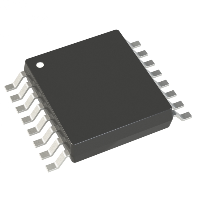
A Comprehensive Guide To S9S12Q12J2VFAE1R Microcontroller IC 16-Bit 16MHz 128KB (128K x 8) FLASH 48-LQFP (7x7)
Payment and disbursement


HCS12 HCS12 Microcontroller IC 16-Bit 16MHz 128KB (128K x 8) FLASH 48-LQFP (7x7)
Introduction
The MC9S12Q128-Family is a 48/52/80 pin Flash-based MCU family, which delivers the power and
flexibility of the 16 Bit core to a whole new range of cost and space sensitive, general purpose Industrial
and Automotive network applications All MC9S12Q128-Familymembers feature standard on-chip
peripherals including a 16-bit central processing unit (CPU12), up to 128K bytes of Flash EEPROM (or
ROM), up to 4K bytes of RAM, an asynchronous serial communications interface (SCI), a serial peripheral
interface (SPI), a 6-channel 16-bit timermodule (TIM), a 4-channel 8-bit pulse width modulator (PWM),
an 8-channel, 10-bit analog-to-digital converter (ADC).
All MC9S12Q128-Family devices feature full 16-bit data paths throughout. The inclusion of a PLL circuit
allows power consumption and performance to be adjusted to suit operational requirements. In addition to
the I/O ports available in each module, up to 10 dedicated I/O port bits are available with wake-up
capability from stop or wait mode. The MC9S12Q128-Family devices are available in 48-, 52-, and 80-pin
QFP packages, with the 80-pin version pin compatible to the HCS12 A, B,, C and D Family derivatives.
Features
• 16-bit HCS12 core:
— HCS12 CPU
– Upward compatible with M68HC11 instruction set
– Interrupt stacking and programmer’s model identical to M68HC11
– Instruction queue
– Enhanced indexed addressing
— MMC (memory map and interface)
— INT (interrupt control)
— BDM (background debug mode)
— DBG12 (enhanced debug12 module, including breakpoints and change-of-flow trace buffer)
— MEBI (multiplexed expansion bus interface) available only in 80-pin package version
• Wake-up interrupt inputs:
— Up to 12 port bits available for wake up interrupt function with digital filtering
• Memory options:
— 32Kbyte ROM or Flash EEPROM (erasable in 512-byte sectors)
64K, 96K, or 128Kbyte ROM or Flash EEPROM (erasable in 1024-byte sectors)
— 1K, 2K, 3K or 4K Byte RAM
• Analog-to-digital converters:
— One 8-channel module with 10-bit resolution
— External conversion trigger capability
— One 1M bit per second, CAN 2.0 A, B software compatible module
— Five receive and three transmit buffers
— Flexible identifier filter programmable as 2 x 32 bit, 4 x 16 bit, or 8 x 8 bit
— Four separate interrupt channels for Rx, Tx, error, and wake-up
— Low-pass filter wake-up function
— Loop-back for self test operation
• Timer module (TIM):
— 6-Channel timer
— Each channel configurable as either input capture or output compare
— Simple PWM mode
— Modulo reset of timer counter
— 16-bit pulse accumulator
— External event counting
— Gated time accumulation
• PWM module:
— Programmable period and duty cycle
— 8-bit 4-channel or 16-bit 2-channel
— Separate control for each pulse width and duty cycle
— Center-aligned or left-aligned outputs
— Programmable clock select logic with a wide range of frequencies
— Fast emergency shutdown input
• Serial interfaces:
— One asynchronous serial communications interface (SCI)
— One synchronous serial peripheral interface (SPI)
• CRG (clock reset generator module)
— Windowed COP watchdog
— Real time interrupt
— Clock monitor
— Pierce or low current Colpitts oscillator
— Phase-locked loop clock frequency multiplier
— Limp home mode in absence of external clock
— Low power 0.5MHz to 16MHz crystal oscillator reference clock
• :Operating frequency
— 16MHz equivalent to 8MHz Bus Speed for single chip
— 16MHz equivalent to 8MHz Bus Speed in expanded bus modes
— Option of 32 MHz equivalent to 16MHz Bus Speed
• Internal 2.5V regulator:
— Supports an input voltage range from 2.97V to 5.5V
— Low power mode capability
— Includes low voltage reset (LVR) circuitry
— Includes low voltage interrupt (LVI) circuitry
• 48-pin LQFP, 52-pin LQFP, or 80-pin QFP package:
— Up to 58 I/O lines with 5V input and drive capability (80-pin package)
— Up to 2 dedicated 5V input only lines (IRQ, XIRQ)
— 5V 8 A/D converter inputs and 5V I/O
• Development support:
— Single-wire background debug™ mode (BDM)
— On-chip hardware breakpoints
— Enhanced DBG12 debug features
Hot Sales
Pricing And ODER
Stock:
0
Price:
$17.16
Quantity:
Shipping Cost
$28.63
PostNL International Mail 11-33
?Unconfirmed payment orders may not be able to deliver the normal cancellation of the order, please communicate with the email to confirm before making the relevant payment ~ Attached email phone number The platform has the right to cancel the unconfirmed payment orders do not need to bear the responsibility of default.
Shipment Date
2025/04/19 AM
Delivery Date
5-10 business days
About Logistics:
?Shipping time will be determined according to the logistics time, there will be differences in the place please understand!
| Sub-Total | $17.16 |
| Shipping: | $28.63 |
| Total | $45.79 |
Please send RFQ , we will respond immediately.
Product:
-
 Afghanistan
-
Afghanistan
-
 Albania
-
 Algeria
-
 American Samoa
-
 Andorra
-
 Angola
-
 Anguilla
-
 Antigua & Barbuda
-
 Argentina
-
 Arizona
-
 Armenia
-
 Aruba
Aruba
-
 Australia
-
 Austria
-
 Azerbaijan
-
 Bahamas
-
 Bahrain
-
 Bangladesh
-
 Barbados
-
 Belarus
-
 Belgium
-
 Belize
-
 Benin
Benin
-
 Bermuda
-
 Bhutan
-
 Bolivia
-
 Bonaire
-
 Bosnia and Herzegovina
-
 Botswana
-
 Brazil
-
 British Virgin Islands
-
 Brunei
-
 Bulgaria
-
 Burkina Faso
-
 Burundi
-
 California
-
 Cambodia
-
 Cameroon
-
 Canada
-
 Cape Verde
-
 Cayman Islands
-
 Central African Republic
-
 Chad
Chad
-
 Chile
Chile
-
 Colombia
-
 Colorado
-
 Congo
Congo
-
 Cook Islands
-
 Costa Rica
-
 Côte d'Ivoire
-
 Croatia
-
 Curaçao
-
 Curacao
-
 Cyprus
-
 Czech Republic
-
 Democratic Republic of Congo
-
Democratic Republic of the Congo
-
 Denmark
-
 Djibouti
-
 Dominica
-
 Dominican Republic
-
 East Timor
-
 Ecuador
-
 Egypt
Egypt
-
 El Salvador
-
 Eritrea
-
 Estonia
-
Eswatini
-
 Ethiopia
-
 Faroe Islands
-
 Fiji
Fiji
-
 Finland
-
 France
-
 French Guiana
-
 French Polynesia
-
 Gabon
Gabon
-
 Gambia
-
 Georgia
-
 Germany
-
 Ghana
Ghana
-
 Gibraltar
-
 Greece
-
 Greenland
-
 Grenada
-
 Guadeloupe
-
 Guam
Guam
-
 Guatemala
-
 Guinea
-
 Guyana
-
 Haiti
Haiti
-
 Honduras
-
 Hong Kong
-
Hong Kong, China
-
 Hungary
-
 Iceland
-
 Idaho
Idaho
-
 India
India
-
 Indonesia
-
 Iraq
Iraq
-
 Ireland
-
 Israel
-
 Italy
Italy
-
Ivory Coast
-
 Jamaica
-
 Japan
Japan
-
 Jordan
-
 Kazakhstan
-
 Kenya
Kenya
-
 Kuwait
-
 Kyrgyzstan
-
 Laos
Laos
-
 Latvia
-
 Lebanon
-
 Lesotho
-
 Liberia
-
 Libya
Libya
-
 Liechtenstein
-
Liechtenstein (Switzerland)
-
 Lithuania
-
 Luxembourg
-
Macao, China
-
 Macau
Macau
-
 Macedonia
-
 Madagascar
-
 Malawi
-
 Malaysia
-
 Maldives
-
 Mali
Mali
-
 Malta
Malta
-
 Marshall Islands
-
 Martinique
-
 Mauritania
-
 Mauritius
-
 Mexico
-
 Micronesia
-
 Moldova
-
 Monaco
-
Monaco (France)
-
 Mongolia
-
 Montenegro
-
 Montserrat
-
 Morocco
-
 Mozambique
-
 Myanmar
-
 Namibia
-
 Nepal
Nepal
-
 Netherlands
-
 Netherlands Antilles
-
 Nevada
-
 New Caledonia
-
 New Zealand
-
 Nicaragua
-
 Niger
Niger
-
 Nigeria
-
North Macedonia
-
 Northern Mariana Islands
-
 Norway
-
 Oman
Oman
-
 Oregon
-
 Other States in US
-
 Pakistan
-
 Palau
Palau
-
Palestinian Authority
-
 Palestinian Territories
-
 Panama
-
 Papua New Guinea
-
 Paraguay
-
 Peru
Peru
-
 Philippines
-
 Poland
-
 Portugal
-
 Puerto Rico
-
 Qatar
Qatar
-
Republic of Moldova
-
Rest of the United States
-
 Réunion
-
Reunion
-
 Romania
-
Rota (Northern Mariana Islands)
-
 Russian
-
Russian Federation
-
 Rwanda
-
Saint Kitts and Nevis
-
 Saint Lucia
-
Saint Maarten (Dutch part)
-
 Saint Martin (French part)
-
 Saint Vincent and the Grenadines
-
Saipan (Northern Mariana Islands)
-
 Samoa
Samoa
-
 San Marino
-
 Saudi Arabia
-
 Senegal
-
 Serbia
-
 Seychelles
-
 Sierra Leone
-
 Singapore
-
 Slovakia
-
 Slovenia
-
Solomon Islands
-
 South Africa
-
 South Korea
-
 Spain
Spain
-
 Sri Lanka
-
 St. Kitts and Nevis
-
 St. Maarten
-
 Suriname
-
 Swaziland (Eswatini)
-
 Sweden
-
 Switzerland
-
 Syria
Syria
-
 Taiwan
-
Taiwan, China
-
 Tajikistan
-
 Tanzania
-
 Thailand
-
Tinian (Northern Mariana Islands)
-
 Togo
Togo
-
 Tonga
Tonga
-
 Trinidad and Tobago
-
 Tunisia
-
 Turkey
-
 Turks and Caicos Islands
-
 Uganda
-
 Ukraine
-
 United Arab Emirates
-
 United Kingdom
-
United Kingdom (Great Britain)
-
 United States
-
 United States Virgin Islands
-
 Uruguay
-
 Utah
Utah
-
 Uzbekistan
-
 Vanuatu
-
 Venezuela
-
 Vietnam
-
 Wallis and Futuna
-
 Washington
-
 Yemen
Yemen
-
 Zambia
-
 Zimbabwe
| Shipping method | Costs | Delivery Time | |
|---|---|---|---|
 SF Express SF Express |
$21.08 | 6-8 business days |


