FIRST ORDER
FREE 10% DISCOUNT


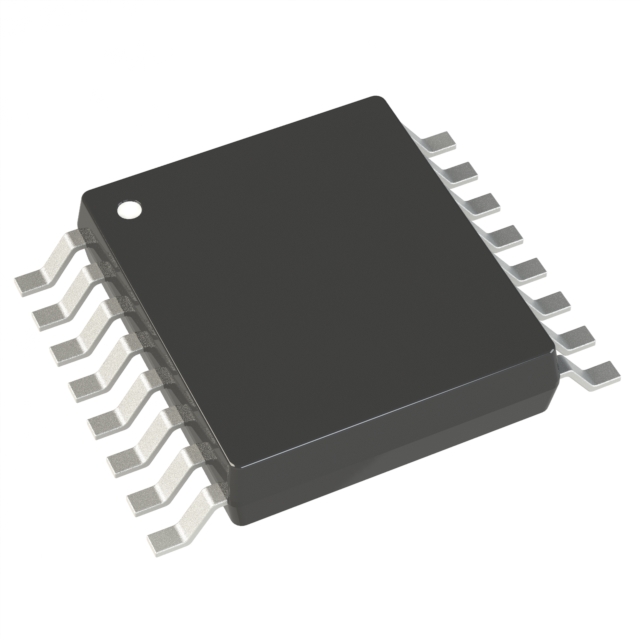
A Comprehensive Guide To S9S12XS128J1VAA Microcontroller IC 16-Bit 40MHz 128KB (128K x 8) FLASH 80-QFP (14x14)
Payment and disbursement


HCS12X HCS12X Microcontroller IC 16-Bit 40MHz 128KB (128K x 8) FLASH 80-QFP (14x14)
MC9S12XS256
Covers MC9S12XS Family
MC9S12XS256
MC9S12XS128
MC9S12XS64
MC9S12XS256
Introduction
The new S12XS family of 16-bit micro controllers is a compatible, reduced version of the S12XE family.
These families provide an easy approach to develop common platforms from low-end to high-end
applications, minimizing the redesign of software and hardware.
Targeted at generic automotive applications and CAN nodes, some typical examples of these applications
are: Body Controllers, Occupant Detection, Door Modules, RKE Receivers, Smart Actuators,Lighting
Modules and Smart Junction Boxes amongst many others.
The S12XS family retains many of the features of the S12XE family including Error Correction Code
(ECC) on Flash memory, a separate Data-Flash Module for code or data storage, a Frequency Modulated
Locked Loop (IPLL) that improves the EMC performance and a fast ATD converter.
s12XS family delivers 32-bit performance with all the advantages and efficiencies ofa 16-bit MCU while
retaining the low cost, power consumption, EMC and code-size efficiency advantages currently enjoyed
by users of Freescale's existing 16-bit S12and S12X MCU families. Like members of other S12X
families, the S12XS family runs 16-bit wide accesses without wait states for all peripherals and memories.
The S12XS family is available in 112-pinLQFP,80-pin QFP,64-pin LQFP package options and maintains
a high level of pin compatibility with the S12XE family. In addition to the I/O ports available in each
module, up to 18 further I/O ports are available with interrupt capability allowing Wake-Up from stop or
wait modes.
The peripheral set includes MSCAN, SPI, two SCIs, an 8-channe1 24-bit periodic interrupt timer, 8-
channel 16-bit Timer, 8-channel PWM and up to 16- channel 12-bit ATD converter.
Software controlled peripheral-to-port routing enables access to a flexible mix of the peripheral modules
in the lower pin count package options.
Features
• 16-bit CPU12X
— Upward compatible with S12 instruction set with the exception of five Fuzzy instructions
(MEM, WAV, WAVR, REV, REVW) which have been removed
— Enhanced indexed addressing
— Access to large data segments independent of PPAGE
• INT (interrupt module)
— Seven levels of nested interrupts
— Flexible assignment of interrupt sources to each interrupt level.
— External non-maskable high priority interrupt (XIRQ)
— The following inputs can act as Wake-up Interrupts
– IRQ and non-maskable XIRQ
– CAN receive pins
– SCI receive pins
– Depending on the package option up to 20 pins on ports J, H and P configurable as rising or
falling edge sensitive
• MMC (module mapping control)
• DBG (debug module)
— Monitoring of CPU bus with tag-type or force-type breakpoint requests
— 64 x 64-bit circular trace buffer captures change-of-flow or memory access information
• BDM (background debug mode)
• OSC_LCP (oscillator)
— Low power loop control Pierce oscillator utilizing a 4MHz to 16MHz crystal
— Good noise immunity
— Full-swing Pierce option utilizing a 2MHz to 40MHz crystal
— Transconductance sized for optimum start-up margin for typical crystals
• IPLL (Internally filtered, frequency modulated phase-locked-loop clock generation)
— No external components required
— Configurable option to spread spectrum for reduced EMC radiation (frequency modulation)
• CRG (clock and reset generation)
— COP watchdog
— Real time interrupt
— Clock monitor
— Fast wake up from STOP in self clock mode
• Memory Options
— 64, 128 and 256 Kbyte Flash
— Flash General Features
– 64 data bits plus 8 syndrome ECC (Error Correction Code) bits allow single bit failure
correction and double fault detection
– Erase sector size 1024 bytes
– Automated program and erase algorithm
– Protection scheme to prevent accidental program or erase
– Security option to prevent unauthorized access
– Sense-amp margin level setting for reads
— 4 and 8 Kbyte Data Flash space
– 16 data bits plus 6 syndrome ECC (Error Correction Code) bits allow single bit failure
correction and double fault detection
– Erase sector size 256 bytes
– Automated program and erase algorithm
— 4, 8 and 12 Kbyte RAM
• 16-channel, 12-bit Analog-to-Digital converter
— 8/10/12 Bit resolution
— 3µs, 10-bit single conversion time
— Left or right justified result data
— External and internal conversion trigger capability
— Internal oscillator for conversion in Stop modes
— Wake from low power modes on analog comparison > or <= match
— Continuous conversion mode
— Multiplexer for 16 analog input channels
— Multiple channel scans
— Pins can also be used as digital I/O
• MSCAN (1 M bit per second, CAN 2.0 A, B software compatible module)
— 1 Mbit per second, CAN 2.0 A, B software compatible module
– Standard and extended data frames
– 0 - 8 bytes data length
– Programmable bit rate up to 1 Mbps
— Five receive buffers with FIFO storage scheme
— Three transmit buffers with internal prioritization
— Flexible identifier acceptance filter programmable as:
– 2 x 32-bit
– 4 x 16-bit
– 8 x 8-bit
— Wake-up with integrated low pass filter option
— Loop back for self test
— Listen-only mode to monitor CAN bus
— Bus-off recovery by software intervention or automatically
— 16-bit time stamp of transmitted/received messages
• TIM (standard timer module)
— 8 x 16-bit channels for input capture or output compare
— 16-bit free-running counter with 8-bit precision prescaler
— 1 x 16-bit pulse accumulator
• PIT (periodic interrupt timer)
— Up to four timers with independent time-out periods
— Time-out periods selectable between 1 and 224 bus clock cycles
— Time-out interrupt and peripheral triggers
— Start of timers can be aligned
• Up to 8 channel x 8-bit or 4 channel x 16-bit Pulse Width Modulator
— Programmable period and duty cycle per channel
— Center- or left-aligned outputs
— Programmable clock select logic with a wide range of frequencies
• Serial Peripheral Interface Module (SPI)
— Configurable for 8 or 16-bit data size
— Full-duplex or single-wire bidirectional
— Double-buffered transmit and receive
— Master or Slave mode
— MSB-first or LSB-first shifting
— Serial clock phase and polarity options
• Two Serial Communication Interfaces (SCI)
— Full-duplex or single wire operation
— Standard mark/space non-return-to-zero (NRZ) format
— Selectable IrDA 1.4 return-to-zero-inverted (RZI) format with programmable pulse widths
— 13-bit baud rate selection
— Programmable character length
— Programmable polarity for transmitter and receiver
— Receive wakeup on active edge
— Break detect and transmit collision detect supporting LIN
• On-Chip Voltage Regulator
— Two parallel, linear voltage regulators with bandgap reference
— Low-voltage detect (LVD) with low-voltage interrupt (LVI)
— Power-on reset (POR) circuit
— Low-voltage reset (LVR)
• Low-power wake-up timer (API)
— Internal oscillator driving a down counter
— Trimmable to +/-5% accuracy
— Time-out periods range from 0.2ms to ~13s with a 0.2ms resolution
• Input/Output
— Up to 91 general-purpose input/output (I/O) pins depending on the package option and 2 inputonly
pins
— Hysteresis and configurable pull up/pull down device on all input pins
— Configurable drive strength on all output pins
• Package Options
— 112-pin low-profile quad flat-pack (LQFP)
— 80-pin quad flat-pack (QFP)
— 64-pin low-profile quad flat-pack (LQFP)
• Operating Conditions
— Wide single Supply Voltage range 3.135 V to 5.5 V at full performance
– Separate supply for internal voltage regulator and I/O allow optimized EMC filtering
— 40MHz maximum CPU bus frequency
— Ambient temperature range –40°C to 125°C
— Temperature Options:
– –40°C to 85°C
– –40°C to 105°C
– –40°C to 125°C
Hot Sales
Pricing And ODER
Stock:
0
Price:
$8.44
Quantity:
Shipping Cost
$28.63
PostNL International Mail 11-33
?Unconfirmed payment orders may not be able to deliver the normal cancellation of the order, please communicate with the email to confirm before making the relevant payment ~ Attached email phone number The platform has the right to cancel the unconfirmed payment orders do not need to bear the responsibility of default.
Shipment Date
2025/04/25 PM
Delivery Date
5-10 business days
About Logistics:
?Shipping time will be determined according to the logistics time, there will be differences in the place please understand!
| Sub-Total | $8.44 |
| Shipping: | $28.63 |
| Total | $37.07 |
Please send RFQ , we will respond immediately.
Product:
-
 Afghanistan
-
Afghanistan
-
 Albania
-
 Algeria
-
 American Samoa
-
 Andorra
-
 Angola
-
 Anguilla
-
 Antigua & Barbuda
-
 Argentina
-
 Arizona
-
 Armenia
-
 Aruba
Aruba
-
 Australia
-
 Austria
-
 Azerbaijan
-
 Bahamas
-
 Bahrain
-
 Bangladesh
-
 Barbados
-
 Belarus
-
 Belgium
-
 Belize
-
 Benin
Benin
-
 Bermuda
-
 Bhutan
-
 Bolivia
-
 Bonaire
-
 Bosnia and Herzegovina
-
 Botswana
-
 Brazil
-
 British Virgin Islands
-
 Brunei
-
 Bulgaria
-
 Burkina Faso
-
 Burundi
-
 California
-
 Cambodia
-
 Cameroon
-
 Canada
-
 Cape Verde
-
 Cayman Islands
-
 Central African Republic
-
 Chad
Chad
-
 Chile
Chile
-
 Colombia
-
 Colorado
-
 Congo
Congo
-
 Cook Islands
-
 Costa Rica
-
 Côte d'Ivoire
-
 Croatia
-
 Curaçao
-
 Curacao
-
 Cyprus
-
 Czech Republic
-
 Democratic Republic of Congo
-
Democratic Republic of the Congo
-
 Denmark
-
 Djibouti
-
 Dominica
-
 Dominican Republic
-
 East Timor
-
 Ecuador
-
 Egypt
Egypt
-
 El Salvador
-
 Eritrea
-
 Estonia
-
Eswatini
-
 Ethiopia
-
 Faroe Islands
-
 Fiji
Fiji
-
 Finland
-
 France
-
 French Guiana
-
 French Polynesia
-
 Gabon
Gabon
-
 Gambia
-
 Georgia
-
 Germany
-
 Ghana
Ghana
-
 Gibraltar
-
 Greece
-
 Greenland
-
 Grenada
-
 Guadeloupe
-
 Guam
Guam
-
 Guatemala
-
 Guinea
-
 Guyana
-
 Haiti
Haiti
-
 Honduras
-
 Hong Kong
-
Hong Kong, China
-
 Hungary
-
 Iceland
-
 Idaho
Idaho
-
 India
India
-
 Indonesia
-
 Iraq
Iraq
-
 Ireland
-
 Israel
-
 Italy
Italy
-
Ivory Coast
-
 Jamaica
-
 Japan
Japan
-
 Jordan
-
 Kazakhstan
-
 Kenya
Kenya
-
 Kuwait
-
 Kyrgyzstan
-
 Laos
Laos
-
 Latvia
-
 Lebanon
-
 Lesotho
-
 Liberia
-
 Libya
Libya
-
 Liechtenstein
-
Liechtenstein (Switzerland)
-
 Lithuania
-
 Luxembourg
-
Macao, China
-
 Macau
Macau
-
 Macedonia
-
 Madagascar
-
 Malawi
-
 Malaysia
-
 Maldives
-
 Mali
Mali
-
 Malta
Malta
-
 Marshall Islands
-
 Martinique
-
 Mauritania
-
 Mauritius
-
 Mexico
-
 Micronesia
-
 Moldova
-
 Monaco
-
Monaco (France)
-
 Mongolia
-
 Montenegro
-
 Montserrat
-
 Morocco
-
 Mozambique
-
 Myanmar
-
 Namibia
-
 Nepal
Nepal
-
 Netherlands
-
 Netherlands Antilles
-
 Nevada
-
 New Caledonia
-
 New Zealand
-
 Nicaragua
-
 Niger
Niger
-
 Nigeria
-
North Macedonia
-
 Northern Mariana Islands
-
 Norway
-
 Oman
Oman
-
 Oregon
-
 Other States in US
-
 Pakistan
-
 Palau
Palau
-
Palestinian Authority
-
 Palestinian Territories
-
 Panama
-
 Papua New Guinea
-
 Paraguay
-
 Peru
Peru
-
 Philippines
-
 Poland
-
 Portugal
-
 Puerto Rico
-
 Qatar
Qatar
-
Republic of Moldova
-
Rest of the United States
-
 Réunion
-
Reunion
-
 Romania
-
Rota (Northern Mariana Islands)
-
 Russian
-
Russian Federation
-
 Rwanda
-
Saint Kitts and Nevis
-
 Saint Lucia
-
Saint Maarten (Dutch part)
-
 Saint Martin (French part)
-
 Saint Vincent and the Grenadines
-
Saipan (Northern Mariana Islands)
-
 Samoa
Samoa
-
 San Marino
-
 Saudi Arabia
-
 Senegal
-
 Serbia
-
 Seychelles
-
 Sierra Leone
-
 Singapore
-
 Slovakia
-
 Slovenia
-
Solomon Islands
-
 South Africa
-
 South Korea
-
 Spain
Spain
-
 Sri Lanka
-
 St. Kitts and Nevis
-
 St. Maarten
-
 Suriname
-
 Swaziland (Eswatini)
-
 Sweden
-
 Switzerland
-
 Syria
Syria
-
 Taiwan
-
Taiwan, China
-
 Tajikistan
-
 Tanzania
-
 Thailand
-
Tinian (Northern Mariana Islands)
-
 Togo
Togo
-
 Tonga
Tonga
-
 Trinidad and Tobago
-
 Tunisia
-
 Turkey
-
 Turks and Caicos Islands
-
 Uganda
-
 Ukraine
-
 United Arab Emirates
-
 United Kingdom
-
United Kingdom (Great Britain)
-
 United States
-
 United States Virgin Islands
-
 Uruguay
-
 Utah
Utah
-
 Uzbekistan
-
 Vanuatu
-
 Venezuela
-
 Vietnam
-
 Wallis and Futuna
-
 Washington
-
 Yemen
Yemen
-
 Zambia
-
 Zimbabwe
| Shipping method | Costs | Delivery Time | |
|---|---|---|---|
 SF Express SF Express |
$21.08 | 6-8 business days |


